

Question: In Section 7.2 we gave the design for a circuit that works as a processor. Give an ASM chart that describes the functionality of this
In Section 7.2 we gave the design for a circuit that works as a processor. Give an ASM chart that describes the functionality of this processor.
Data From Section 7.2
A second example of a digital system like the one in Figure 7.2 is shown in Figure 7.9. It has four n-bit registers, R0, . . . , R3, that are connected to the bus with tri-state drivers. External data can be loaded into the registers from the n-bit Data input, which is connected to the bus using tri-state drivers enabled by the Extern control signal. The system also includes an adder/subtractor module. One of its data inputs is provided by an n-bit register, A, that is attached to the bus, while the other data input, B, is directly connected to the bus. If the Add Sub signal has the value 0, the module generates the sum A + B; if Add Sub = 1, the module generates the difference A − B. To perform the subtraction, we assume that the adder/subtractor includes the required XOR gates to form the 2’s complement of B, as discussed in Section 3.3. The register G stores the output produced by the adder/subtractor.
The A and G registers are controlled by the signals Ain, Gin, and Gout .
The system in Figure 7.9 can perform various functions, depending on the design of the control circuit. As an example, we will design a control circuit that can perform the four operations listed in Table 7.1. The left column in the table shows the name of an operation and its operands; the right column indicates the function performed in the operation. For
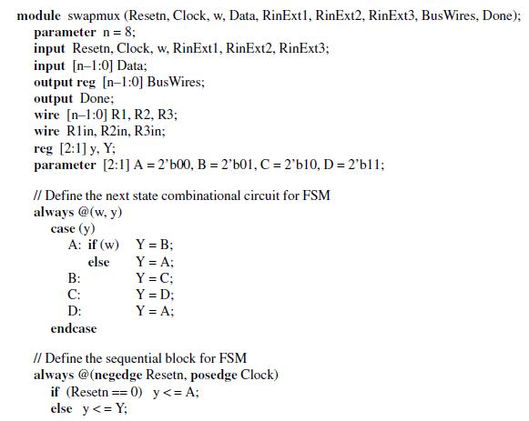
![[n-1:0] Data; output reg [n-1:0] Bus Wires; output Done; wire [n-1:0] R1,](https://dsd5zvtm8ll6.cloudfront.net/si.question.images/images/question_images/1662/4/4/1/1586316d6c66f6bf1662441160110.jpg)
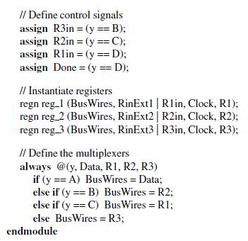
module swapmux (Resetn, Clock, w, Data, RinExt1, RinExt2, RinExt3, Bus Wires, Done); parameter n = 8; input Resetn, Clock, w, RinExt1, RinExt2, RinExt3; input [n-1:0] Data; output reg [n-1:0] Bus Wires; output Done; wire [n-1:0] R1, R2, R3; wire R1in, R2in, R3in; reg [2:1] y, Y; parameter [2:1] A = 2'b00, B = 2'b01, C = 2'b10, D = 2'bll; // Define the next state combinational circuit for FSM always @(w, y) case (y) A: if (w) else B: C: D: endcase Y = B; Y = A; Y = C; Y =D; Y = A; // Define the sequential block for FSM always @(negedge Resetn, posedge Clock) if (Resetn == 0) y
Step by Step Solution
3.47 Rating (163 Votes )
There are 3 Steps involved in it
ASM Chart for the Processor Inputs Reset Asynchronous res... View full answer

Get step-by-step solutions from verified subject matter experts