

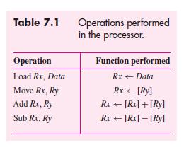
Question: In Section 7.2 we designed a processor that performs the operations listed in Table 7.1. Design a modified circuit that performs an additional operation Swap
In Section 7.2 we designed a processor that performs the operations listed in Table 7.1. Design a modified circuit that performs an additional operation Swap Rx, Ry. This operation swaps the contents of registers Rx and Ry. Use three bits f2 f1 f0 to represent the input F shown in Figure 7.11 because there are now five operations, rather than four. Add a new register, named Tmp, into the system, to be used for temporary storage during the swap operation. Show logic expressions for the outputs of the control circuit, as was done in Section 7.2.
Data From Section 7.2
![Data Rx + [Ry] Rx+ [Rx] + [Ry] Rx - [Rx]-[Ry]](https://dsd5zvtm8ll6.cloudfront.net/si.question.images/images/question_images/1662/3/8/2/2966315f0d8de1d31662382294710.jpg)
Table 7.1 Operation Load Rx, Data Move Rx, Ry Add Rx, Ry Sub Rx, Ry Operations performed in the processor. Function performed Rx + Data Rx + [Ry] Rx+ [Rx] + [Ry] Rx - [Rx]-[Ry]
Step by Step Solution
3.55 Rating (176 Votes )
There are 3 Steps involved in it
To design a modified circuit that performs an additional swap operation using a temporary register Tmp lets follow these steps 1 Add OpCode Since the ... View full answer

Get step-by-step solutions from verified subject matter experts