

Question: 1 2R, 2nR, C, APPENDIX II: Standard Values Resistors Standard Values of Commercially Available Resistors Ohms (0) Kilo Ohms (ko) Mega Ohms (MO) 10 11
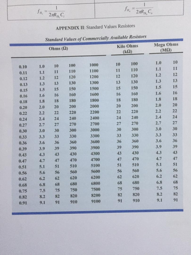
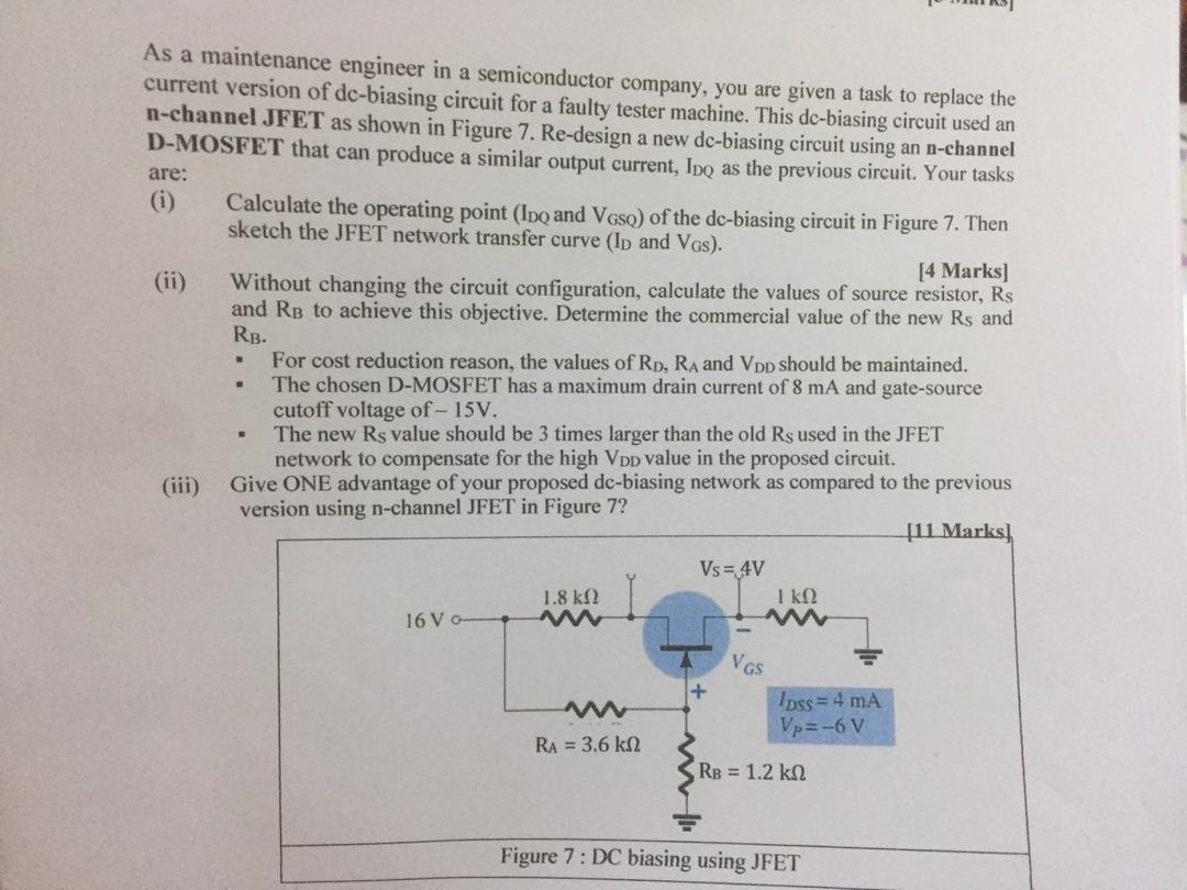
1 2R, 2nR, C, APPENDIX II: Standard Values Resistors Standard Values of Commercially Available Resistors Ohms (0) Kilo Ohms (ko) Mega Ohms (MO) 10 11 10 11 12 12 13 0.10 0.11 0.12 0.13 0.15 0.16 0.18 0.20 0.22 0.24 0.27 0.30 13 15 16 18 20 1.0 1.1 1.2 1.3 1.5 1.6 1.8 2.0 2.2 2.4 2.7 3.0 3.3 3.6 3.9 4.3 4.7 5.1 5.6 6.2 6.8 7.5 8.2 9.1 100 110 120 130 150 160 180 200 220 240 270 300 330 360 390 22 10 11 12 13 15 16 18 20 22 24 27 30 33 36 39 43 47 51 56 62 68 75 1000 1100 1200 1300 1500 1600 1800 2000 2200 2400 2700 3000 3300 3600 3900 4300 4700 5100 5600 6200 6800 7500 8200 9100 24 27 30 33 100 110 120 130 150 160 180 200 220 240 270 300 330 360 390 430 470 510 560 620 680 750 820 910 1.0 1.1 1.2 1.3 1.5 1.6 1.8 2.0 2.2 2.4 2.7 3.0 3.3 3.6 3.9 4.3 4.7 5.1 5.6 6.2 6.8 7.5 8.2 9.1 0.33 36 15 16 18 20 22 24 27 30 33 36 39 43 47 51 56 62 68 75 82 91 39 430 0.36 0.39 0.43 0.47 0.51 0.56 0.62 0.68 0.75 0.82 0.91 43 470 510 560 620 680 750 820 910 47 51 56 62 68 75 82 91 82 91 As a maintenance engineer in a semiconductor company, you are given a task to replace the current version of de-biasing circuit for a faulty tester machine. This de-biasing circuit used an n-channel JFET as shown in Figure 7. Re-design a new dc-biasing circuit using an n-channel D-MOSFET that can produce a similar output current, Ipo as the previous circuit. Your tasks are: Calculate the operating point (Ido and Vgso) of the dc-biasing circuit in Figure 7. Then sketch the JFET network transfer curve (Ip and Vgs). [4 Marks] Without changing the circuit configuration, calculate the values of source resistor, Rs and RB to achieve this objective. Determine the commercial value of the new Rs and RB. For cost reduction reason, the values of Rp, RA and Vpp should be maintained. The chosen D-MOSFET has a maximum drain current of 8 mA and gate-source cutoff voltage of -15V. The new Rs value should be 3 times larger than the old Rs used in the JFET network to compensate for the high Vpp value in the proposed circuit. Give ONE advantage of your proposed dc-biasing network as compared to the previous version using n-channel JFET in Figure 7? [11 Marks! Vs = 4V 1.8 k 2 I KO 16 VO- (iii) Vas + IDss = 4 mA Vp=-6 V RA = 3.6 k 2 RB = 1.2 k2 Figure 7: DC biasing using JFET 1 2R, 2nR, C, APPENDIX II: Standard Values Resistors Standard Values of Commercially Available Resistors Ohms (0) Kilo Ohms (ko) Mega Ohms (MO) 10 11 10 11 12 12 13 0.10 0.11 0.12 0.13 0.15 0.16 0.18 0.20 0.22 0.24 0.27 0.30 13 15 16 18 20 1.0 1.1 1.2 1.3 1.5 1.6 1.8 2.0 2.2 2.4 2.7 3.0 3.3 3.6 3.9 4.3 4.7 5.1 5.6 6.2 6.8 7.5 8.2 9.1 100 110 120 130 150 160 180 200 220 240 270 300 330 360 390 22 10 11 12 13 15 16 18 20 22 24 27 30 33 36 39 43 47 51 56 62 68 75 1000 1100 1200 1300 1500 1600 1800 2000 2200 2400 2700 3000 3300 3600 3900 4300 4700 5100 5600 6200 6800 7500 8200 9100 24 27 30 33 100 110 120 130 150 160 180 200 220 240 270 300 330 360 390 430 470 510 560 620 680 750 820 910 1.0 1.1 1.2 1.3 1.5 1.6 1.8 2.0 2.2 2.4 2.7 3.0 3.3 3.6 3.9 4.3 4.7 5.1 5.6 6.2 6.8 7.5 8.2 9.1 0.33 36 15 16 18 20 22 24 27 30 33 36 39 43 47 51 56 62 68 75 82 91 39 430 0.36 0.39 0.43 0.47 0.51 0.56 0.62 0.68 0.75 0.82 0.91 43 470 510 560 620 680 750 820 910 47 51 56 62 68 75 82 91 82 91 As a maintenance engineer in a semiconductor company, you are given a task to replace the current version of de-biasing circuit for a faulty tester machine. This de-biasing circuit used an n-channel JFET as shown in Figure 7. Re-design a new dc-biasing circuit using an n-channel D-MOSFET that can produce a similar output current, Ipo as the previous circuit. Your tasks are: Calculate the operating point (Ido and Vgso) of the dc-biasing circuit in Figure 7. Then sketch the JFET network transfer curve (Ip and Vgs). [4 Marks] Without changing the circuit configuration, calculate the values of source resistor, Rs and RB to achieve this objective. Determine the commercial value of the new Rs and RB. For cost reduction reason, the values of Rp, RA and Vpp should be maintained. The chosen D-MOSFET has a maximum drain current of 8 mA and gate-source cutoff voltage of -15V. The new Rs value should be 3 times larger than the old Rs used in the JFET network to compensate for the high Vpp value in the proposed circuit. Give ONE advantage of your proposed dc-biasing network as compared to the previous version using n-channel JFET in Figure 7? [11 Marks! Vs = 4V 1.8 k 2 I KO 16 VO- (iii) Vas + IDss = 4 mA Vp=-6 V RA = 3.6 k 2 RB = 1.2 k2 Figure 7: DC biasing using JFET
Step by Step Solution
There are 3 Steps involved in it

Get step-by-step solutions from verified subject matter experts