

Question: 1. Draw the multiple-level NOR circuit for the following expression The procedure in the design of multilevel circuits: 1. Convert all AND gates to NAND
1. Draw the multiple-level NOR circuit for the following expression
The procedure in the design of multilevel circuits:
1. Convert all AND gates to NAND gates with AND-invert graphic symbols.
2. Convert all OR gates to NAND gates with invert-OR graphic symbols.
3. Check all the bubbles in the diagram.
1) F = BC(D + C)A + (BC' + DE') + BD
2) F=(A+B+C+D)(A+B+C+E)(A+B+C+F)
2. Draw the multiple-level NAND circuit for the following expression:
Multilevel NAND Circuits The procedure in the design of multilevel circuits: 1. Convert all AND gates to NAND gates with AND-invert graphic symbols. 2. Convert all OR gates to NAND gates with invert-OR graphic symbols. 3. Check all the bubbles in the diagram.
1) F = w(x + y + z) + xyz
2) WXYZ+VXYZ+UXYZ
.......
Drawing in the same way as the picture
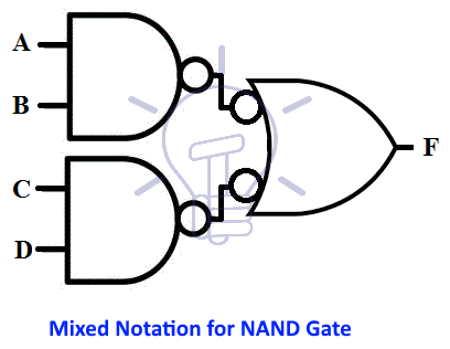
Dag F C Da D- Mixed Notation for NAND Gate
Step by Step Solution
There are 3 Steps involved in it

Get step-by-step solutions from verified subject matter experts