Question: i keep getting errors when i make this controller and it is really frustrating me could someone please show me the correct way to implement
i keep getting errors when i make this controller and it is really frustrating me could someone please show me the correct way to implement this? i will for sure upvote.i need the design schematics as well as the truth table for it. thank you!

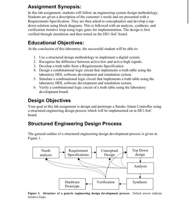
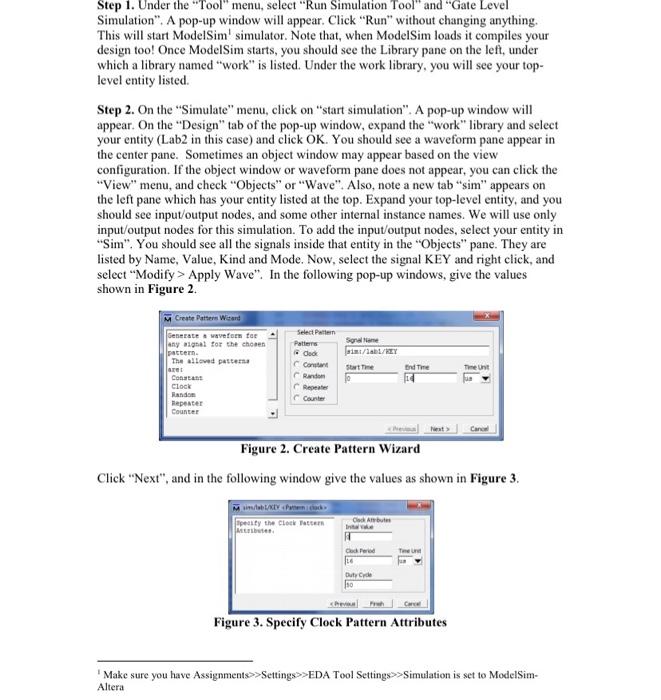
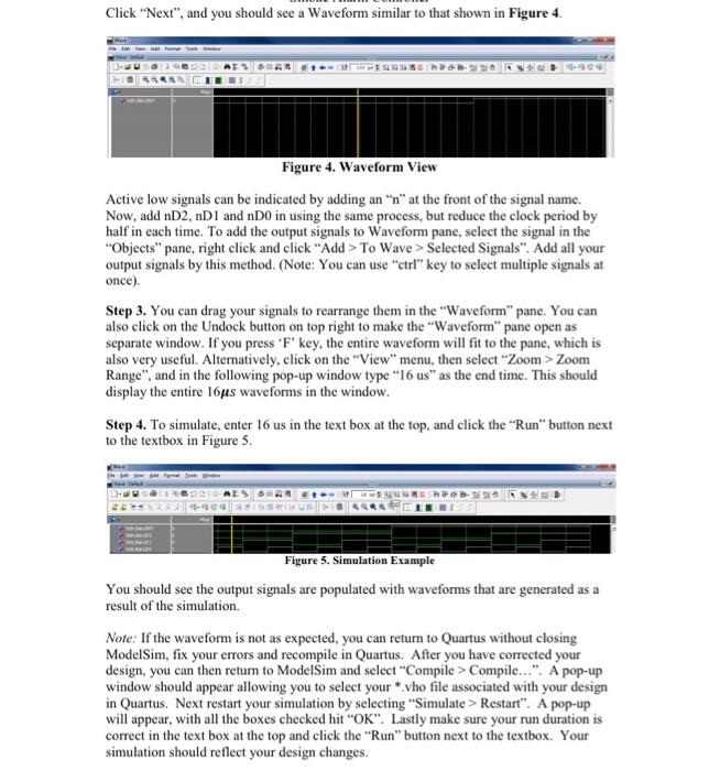
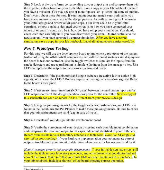
Assignment Synopsis: In this lab assignment, students will follow an engineering system design methodology. Students are given a description of the customer's needs and are presented with a Requirements Specification. They are then asked to conceptualize and develop a top- down solution using block diagrams. This is followed with an analysis, synthesis, and verification iterative loop using logic gates for implementation. The design is first verified through simulation and then tested on the DE1-SOC board. Educational Objectives: At the conclusion of this laboratory, the successful student will be able to: 1. Use a structured design methodology to implement a digital system. 2. Recognize the difference between active-low and active-high signals. 3. Develop a truth table from a Requirements Specification. 4. Design a combinational logic circuit that implements a truth table using the laboratory HDL software development and simulation system. 5. Simulate a combinational logic circuit that implements a truth table using the laboratory HDL software development and simulation system. 6. Verify a combinational logic circuit of a truth table using the laboratory development board. Design Objectives Your goal in this lab assignment is design and prototype a Smoke Alarm Controller using a structured engineering design process which will be implemented on ta DE1-SOC board. Structured Engineering Design Process The general outline of a structured engineering design development process is given in Figure 1. Needs analysis Requirement Specifications Conceptual Design Top Down design Analysis Verification Synthesis Hardware Prototype Figure 1. Structure of a generic engineering design development process. Dotted arrows indicate iterative loops. Before developing a design, the engineer must first convert the customer's needs into a requirements specification. This is known as a "Needs Analysis." Let's look at the needs analysis for our problem. Needs Analysis A customer needs a controller for a building smoke alarm system. We need to ask the customer some questions to convert this "need" into a requirements specification. This is known as a "Needs Analysis." We'll walk through this step together. Q: How many rooms do you want to be covered by the system? R: Three rooms Q: Do you wish the system to automatically set off a sprinkler system? R: Not always. Our old system was always giving us false alarms. I would hate to have water everywhere, if it was necessary. Q: I think our system will be more reliable. However, what if we designed the system to activate the sprinklers, if say, we detected smoke in two of the three rooms? R: Yes, that would be good. Q: Would you like a dialer feature to automatically call the Fire Department? R: Yes. Can it be activated if any of the rooms detected smoke? Q: Sure. Are there any other features you would like? R: Yes, I assume you'll include an audible alarm when smoke is detected? Q: Of course. Is there anything else? R: Yes, can you add a manual key override that allows us to turn on the alarm and call the fire department even if smoke is not detected. Q: No problem. Anything else? A: No, but I'll call you if I think of something later. Requirements Specification. Based on our conversation with our customer, we are ready to develop a Requirements Specification. In practice, you may need to go back to the customer several times before you truly understand your customer's needs. For this design, we determine that our building is to be protected by a smoke alarm system that has three smoke detectors one for each room), a manager's override key, a sprinkler, an alarm, and an automatic telephone dialer. The sprinkler is to be activated if any two of the three smoke detectors detect smoke. The alarm should sound, and the fire department should be called whenever any of the smoke detectors detect smoke. The manager's override key can also turn on the alarm and activate the automatic dialer. We will purchase several items as commercial off-the-shelf (COTS) components: the smoke detectors, the key override, the sprinkler system, and the auto-dialer. After examining the specifications (i.e., specs) of each of these devices, we find that each smoke detector has a single active-low output, which we will call that is asserted whenever it detects smoke particles. The manager's override key has an active-high output that we'll call KEY. The sprinkler has an active-low input, which we'll call SPK, that must be asserted to turn on the sprinkler. The alarm will sound whenever its active- high input signal, called ARM, is asserted. The telephone dialer initiates a call whenever its active-high input signal, called DIAL is asserted. Based on this description, we need to develop a list of input and output signals needed by the controller. For each signal, indicate its name, whether it is an input or an output, and the type of encoding (i.e., active high or active low). If you have more than one of the same type of inputs or outputs, use a numerical index to uniquely identify each signal and complement any signal name that is actively low. Typically, we start numbering signals from 0. So, use DO as the output from the first smoke detector, D1 as the output from the second smoke detector, and D2 as the output from the third smoke detector. We are now ready for the top-level design. Pre-Lab Preparation: Note: Write up your pre-lab assignment in your laboratory notebook. Part 1. Top-Level Design Step 1. Our job is to design a control circuit for a smoke alarm system. First, how does this controller component fit into the overall system? Draw a schematic (block diagram) that includes a block (labeled rectangle) for each of the major components of the system. Include a separate block for each smoke detector, one for the controller and one each for the alarm and sprinkler system. We'll represent the manager's key as a direct input. Now, draw a line for each connection between blocks. Generally, you want your signal flow to move from the left side of your diagram to the right side. Step 2. Place labels on each block and on each signal connection. Use the same names used in the Requirements Specification. Step 3. For each of your signals, add arrowheads to your lines showing the direction of information flow. Include a sketch of your block diagram in your lab notebook. Step 4. The controller should take all the available input signals and generate the output signals to meet the design requirements. Based on the Requirements Specification, develop a truth table for your design. You should have four inputs, DO, D1, and D2, KEY and three outputs, SPK, DIAL and ARM. Include your truth table in your lab notebook. Step 5. For each output, develop a Sum-of-Products (SOP) Boolean equation that relates each output to your four inputs. Show your work and give the final equation in your lab notebook. Step 6. Using 2-, 3-, and 4-input basic logic gates, draw a digital logic circuit for each equation developed in Step 5. Depending on the complexity of your circuit, these drawings may be large. However, if you wish, you may "minimize" each expression using minimization techniques covered in class or in your textbook. Include the sketch of your digital logic circuit in your lab notebook. Step 7. In the lab, you will use the DE1-SoC to prototype your design. Toggle switches will be utilized to emulate the output from the smoke detectors and a pushbutton for the manager's key. LEDs will be used to indicate if the sprinkler, alarm, or dialer system have been activated. Review the DE1-SoC User's Guide and identify the name and FPGA pins for three toggle switches, one push button, and three LEDs to use in your design. Record this information in your lab notebook. In-Lab Procedure After your TA checks your pre-lab work, coordinate with your lab partner (if any) to agree on any necessary changes and begin the implementation. Part 1. Implementation Now that you've developed your logic circuits on paper, create a schematic using the lab HDL development system to simulate and synthesize your design. Step 1. Create a new folder and a new project and schematic file for your controller circuit, using meaningful names. Create input and output pins for each signals. However, don't assign them to specific FGPA pins yet. Step 2. Using Quartus, click the button that looks like an "AND" gate from the toolbar at the left. This will bring up the "Symbol" dialog. In the "Libraries" area, expand "primitives" and then "logic" and you will see a list of available gates. If you click on the gate name, you will see a picture of it to the right in the dialog. There are a variety of possible gates, and combinations of gates, that could be used to meet your specifications. If going through this list gives you any new ideas for your design, you can go back and redesign your circuits. After selecting the gate you want to try, click "OK", and place it in your design. Repeat this process for each gate you want to create. Step 3. Connect the gates appropriately to the inputs and outputs according to your design. Step 4. Now your design is complete. Save your schematic and compile it. Don't worry about pin assignments yet (they are not needed for compilation). Save a screen-capture of your schematic and a screen capture showing successful compilation to include in your lab report. Part 2. Simulation Testing In this part of the assignment, we walk you through the process for testing your design with the simulator, to make sure it will produce the outputs you expect. We will be using ModelSim with Quartus to perform the simulation. Step 1. Under the "Tool" menu, select "Run Simulation Tool" and "Gate Level Simulation". A pop-up window will appear. Click "Run" without changing anything. This will start ModelSim' simulator. Note that, when ModelSim loads it compiles your design too! Once ModelSim starts, you should see the Library pane on the left, under which a library named "work" is listed. Under the work library, you will see your top- level entity listed. Step 2. On the "Simulate" menu, click on "start simulation". A pop-up window will appear. On the "Design" tab of the pop-up window, expand the "work" library and select your entity (Lab2 in this case) and click OK. You should see a waveform pane appear in the center pane. Sometimes an object window may appear based on the view configuration. If the object window or waveform pane does not appear, you can click the "View" menu, and check "Objects" or "Wave". Also, note a new tab "sim" appears on the left pane which has your entity listed at the top. Expand your top-level entity, and you should see input/output nodes, and some other internal instance names. We will use only input/output nodes for this simulation. To add the input/output nodes, select your entity in "Sim". You should see all the signals inside that entity in the "Objects" pane. They are listed by Name, Value, Kind and Mode. Now, select the signal KEY and right click, and select "Modify > Apply Wave". In the following pop-up windows, give the values shown in Figure 2. M Create Pattern Wizard Generate a waveform for any signal for the chosen pattern. Select Pattern Patterns Signal Name 11/11/KEY Clock The allowed patterns are: Constant Start Time End Time Time Unit Randon Constant Clock Randon Repeater Counter Repeater Counter Figure 2. Create Pattern Wizard Click "Next", and in the following window give the values as shown in Figure 3. Mm/ab/KEY Pancak Specify the Clock Pattern Attributes Clock Ital vake Cock Frid Duty Cy Carca Figure 3. Specify Clock Pattern Attributes Make sure you have Assignments>>Settings>>EDA Tool Settings>>Simulation is set to ModelSim- Altera Click "Next", and you should see a Waveform similar to that shown in Figure 4. 4-404 Figure 4. Waveform View Active low signals can be indicated by adding an "n" at the front of the signal name. Now, add nD2, nD1 and nD0 in using the same process, but reduce the clock period by half in each time. To add the output signals to Waveform pane, select the signal in the "Objects" pane, right click and click "Add > To Wave> Selected Signals". Add all your output signals by this method. (Note: You can use "ctrl" key to select multiple signals at once). Step 3. You can drag your signals to rearrange them in the "Waveform" pane. You can also click on the Undock button on top right to make the "Waveform" pane open as separate window. If you press 'F' key, the entire waveform will fit to the pane, which is also very useful. Alternatively, click on the "View" menu, then select "Zoom> Zoom Range", and in the following pop-up window type "16 us" as the end time. This should display the entire 16s waveforms in the window. Step 4. To simulate, enter 16 us in the text box at the top, and click the "Run" button next to the textbox in Figure 5. G HOOD ANLED WE WID ARAINHI Figure 5. Simulation Example You should see the output signals are populated with waveforms that are generated as a result of the simulation. Note: If the waveform is not as expected, you can return to Quartus without closing ModelSim, fix your errors and recompile in Quartus. After you have corrected your design, you can then return to ModelSim and select "Compile > Compile...". A pop-up window should appear allowing you to select your *.vho file associated with your design in Quartus. Next restart your simulation by selecting "Simulate> Restart". A pop-up will appear, with all the boxes checked hit "OK". Lastly make sure your run duration is correct in the text box at the top and click the "Run" button next to the textbox. Your simulation should reflect your design changes. SUNUKCNFOD-22 Step 5. Look at the waveforms corresponding to your output pins and compare them with the expected values based on your truth table. Save a copy in your lab notebook (even if you have a mistake). You may see one or more "spikes" or "glitches" in some of outputs. Don't worry about these for now. If your output does not match your truth table, you have made an error somewhere in the design process. As outlined in Figure 1, return to your initial design and review all of your steps. Your error could be in your initial equations, or how you have designed your circuits, or how you have connected your inputs or outputs. It could also be in how you have setup your simulation. You should check each step carefully until you have discovered your error. Do not continue to the next step until you have generated a correct simulation. After you have a correct simulation, save a copy in your lab notebook. Label all lab notebook entries carefully. Part 3. Prototype Testing For this part, we will use the development board to implement a prototype of the system. Instead of using the off-the-shelf components, we will use board switches and displays on the board to test our controller. Use the toggle switches to simulate the inputs from the smoke detectors and use a pushbutton to simulate the input from the manager's key. Use LEDs to represent the outputs to the sprinkler, alarm, and dialer. Step 1. Determine if the pushbuttons and toggle switches are active-low or active-high signals. What about the LEDs? Do they require active-high or active-low signals? Refer to the board's user guide. Step 2. If necessary, insert inverters (NOT gates) between the pushbutton input and/or LED outputs to match the design specifications given for the controller. Save a copy of this schematic for your lab report if it is different from your previous design. Step 3. Using the pin assignments for the toggle switches, push buttons, and LEDs you found in the Prelab, use the Pin Planner to make those pin assignments. Be sure to check that your pin assignments are valid (e.g. in case of typos). Step 4. Download your design into the development board. Step 5. Verify the correctness of your design by testing each possible input combination and comparing the observed output to the expected output identified in your truth table. Record your results in your laboratory notebook in table form. Have the TA verify and sign-off on your readings. If your hardware implementation does not generate correct outputs, troubleshoot your circuit to determine where you error has occurred and fix it. Hint: A common error is incorrect pin assignments. If your initial design had errors, still include the table in your laboratory notebook, and write down what you did to find and correct the errors. Make sure that your final table of experimental results is included. In your lab notebook, include a photo(s) of the board showing correct operation. 2 See Appendix A Laboratory Report Follow the Laboratory Report template when writing your lab report. END OF DOCUMENT Assignment Synopsis: In this lab assignment, students will follow an engineering system design methodology. Students are given a description of the customer's needs and are presented with a Requirements Specification. They are then asked to conceptualize and develop a top- down solution using block diagrams. This is followed with an analysis, synthesis, and verification iterative loop using logic gates for implementation. The design is first verified through simulation and then tested on the DE1-SOC board. Educational Objectives: At the conclusion of this laboratory, the successful student will be able to: 1. Use a structured design methodology to implement a digital system. 2. Recognize the difference between active-low and active-high signals. 3. Develop a truth table from a Requirements Specification. 4. Design a combinational logic circuit that implements a truth table using the laboratory HDL software development and simulation system. 5. Simulate a combinational logic circuit that implements a truth table using the laboratory HDL software development and simulation system. 6. Verify a combinational logic circuit of a truth table using the laboratory development board. Design Objectives Your goal in this lab assignment is design and prototype a Smoke Alarm Controller using a structured engineering design process which will be implemented on ta DE1-SOC board. Structured Engineering Design Process The general outline of a structured engineering design development process is given in Figure 1. Needs analysis Requirement Specifications Conceptual Design Top Down design Analysis Verification Synthesis Hardware Prototype Figure 1. Structure of a generic engineering design development process. Dotted arrows indicate iterative loops. Before developing a design, the engineer must first convert the customer's needs into a requirements specification. This is known as a "Needs Analysis." Let's look at the needs analysis for our problem. Needs Analysis A customer needs a controller for a building smoke alarm system. We need to ask the customer some questions to convert this "need" into a requirements specification. This is known as a "Needs Analysis." We'll walk through this step together. Q: How many rooms do you want to be covered by the system? R: Three rooms Q: Do you wish the system to automatically set off a sprinkler system? R: Not always. Our old system was always giving us false alarms. I would hate to have water everywhere, if it was necessary. Q: I think our system will be more reliable. However, what if we designed the system to activate the sprinklers, if say, we detected smoke in two of the three rooms? R: Yes, that would be good. Q: Would you like a dialer feature to automatically call the Fire Department? R: Yes. Can it be activated if any of the rooms detected smoke? Q: Sure. Are there any other features you would like? R: Yes, I assume you'll include an audible alarm when smoke is detected? Q: Of course. Is there anything else? R: Yes, can you add a manual key override that allows us to turn on the alarm and call the fire department even if smoke is not detected. Q: No problem. Anything else? A: No, but I'll call you if I think of something later. Requirements Specification. Based on our conversation with our customer, we are ready to develop a Requirements Specification. In practice, you may need to go back to the customer several times before you truly understand your customer's needs. For this design, we determine that our building is to be protected by a smoke alarm system that has three smoke detectors one for each room), a manager's override key, a sprinkler, an alarm, and an automatic telephone dialer. The sprinkler is to be activated if any two of the three smoke detectors detect smoke. The alarm should sound, and the fire department should be called whenever any of the smoke detectors detect smoke. The manager's override key can also turn on the alarm and activate the automatic dialer. We will purchase several items as commercial off-the-shelf (COTS) components: the smoke detectors, the key override, the sprinkler system, and the auto-dialer. After examining the specifications (i.e., specs) of each of these devices, we find that each smoke detector has a single active-low output, which we will call that is asserted whenever it detects smoke particles. The manager's override key has an active-high output that we'll call KEY. The sprinkler has an active-low input, which we'll call SPK, that must be asserted to turn on the sprinkler. The alarm will sound whenever its active- high input signal, called ARM, is asserted. The telephone dialer initiates a call whenever its active-high input signal, called DIAL is asserted. Based on this description, we need to develop a list of input and output signals needed by the controller. For each signal, indicate its name, whether it is an input or an output, and the type of encoding (i.e., active high or active low). If you have more than one of the same type of inputs or outputs, use a numerical index to uniquely identify each signal and complement any signal name that is actively low. Typically, we start numbering signals from 0. So, use DO as the output from the first smoke detector, D1 as the output from the second smoke detector, and D2 as the output from the third smoke detector. We are now ready for the top-level design. Pre-Lab Preparation: Note: Write up your pre-lab assignment in your laboratory notebook. Part 1. Top-Level Design Step 1. Our job is to design a control circuit for a smoke alarm system. First, how does this controller component fit into the overall system? Draw a schematic (block diagram) that includes a block (labeled rectangle) for each of the major components of the system. Include a separate block for each smoke detector, one for the controller and one each for the alarm and sprinkler system. We'll represent the manager's key as a direct input. Now, draw a line for each connection between blocks. Generally, you want your signal flow to move from the left side of your diagram to the right side. Step 2. Place labels on each block and on each signal connection. Use the same names used in the Requirements Specification. Step 3. For each of your signals, add arrowheads to your lines showing the direction of information flow. Include a sketch of your block diagram in your lab notebook. Step 4. The controller should take all the available input signals and generate the output signals to meet the design requirements. Based on the Requirements Specification, develop a truth table for your design. You should have four inputs, DO, D1, and D2, KEY and three outputs, SPK, DIAL and ARM. Include your truth table in your lab notebook. Step 5. For each output, develop a Sum-of-Products (SOP) Boolean equation that relates each output to your four inputs. Show your work and give the final equation in your lab notebook. Step 6. Using 2-, 3-, and 4-input basic logic gates, draw a digital logic circuit for each equation developed in Step 5. Depending on the complexity of your circuit, these drawings may be large. However, if you wish, you may "minimize" each expression using minimization techniques covered in class or in your textbook. Include the sketch of your digital logic circuit in your lab notebook. Step 7. In the lab, you will use the DE1-SoC to prototype your design. Toggle switches will be utilized to emulate the output from the smoke detectors and a pushbutton for the manager's key. LEDs will be used to indicate if the sprinkler, alarm, or dialer system have been activated. Review the DE1-SoC User's Guide and identify the name and FPGA pins for three toggle switches, one push button, and three LEDs to use in your design. Record this information in your lab notebook. In-Lab Procedure After your TA checks your pre-lab work, coordinate with your lab partner (if any) to agree on any necessary changes and begin the implementation. Part 1. Implementation Now that you've developed your logic circuits on paper, create a schematic using the lab HDL development system to simulate and synthesize your design. Step 1. Create a new folder and a new project and schematic file for your controller circuit, using meaningful names. Create input and output pins for each signals. However, don't assign them to specific FGPA pins yet. Step 2. Using Quartus, click the button that looks like an "AND" gate from the toolbar at the left. This will bring up the "Symbol" dialog. In the "Libraries" area, expand "primitives" and then "logic" and you will see a list of available gates. If you click on the gate name, you will see a picture of it to the right in the dialog. There are a variety of possible gates, and combinations of gates, that could be used to meet your specifications. If going through this list gives you any new ideas for your design, you can go back and redesign your circuits. After selecting the gate you want to try, click "OK", and place it in your design. Repeat this process for each gate you want to create. Step 3. Connect the gates appropriately to the inputs and outputs according to your design. Step 4. Now your design is complete. Save your schematic and compile it. Don't worry about pin assignments yet (they are not needed for compilation). Save a screen-capture of your schematic and a screen capture showing successful compilation to include in your lab report. Part 2. Simulation Testing In this part of the assignment, we walk you through the process for testing your design with the simulator, to make sure it will produce the outputs you expect. We will be using ModelSim with Quartus to perform the simulation. Step 1. Under the "Tool" menu, select "Run Simulation Tool" and "Gate Level Simulation". A pop-up window will appear. Click "Run" without changing anything. This will start ModelSim' simulator. Note that, when ModelSim loads it compiles your design too! Once ModelSim starts, you should see the Library pane on the left, under which a library named "work" is listed. Under the work library, you will see your top- level entity listed. Step 2. On the "Simulate" menu, click on "start simulation". A pop-up window will appear. On the "Design" tab of the pop-up window, expand the "work" library and select your entity (Lab2 in this case) and click OK. You should see a waveform pane appear in the center pane. Sometimes an object window may appear based on the view configuration. If the object window or waveform pane does not appear, you can click the "View" menu, and check "Objects" or "Wave". Also, note a new tab "sim" appears on the left pane which has your entity listed at the top. Expand your top-level entity, and you should see input/output nodes, and some other internal instance names. We will use only input/output nodes for this simulation. To add the input/output nodes, select your entity in "Sim". You should see all the signals inside that entity in the "Objects" pane. They are listed by Name, Value, Kind and Mode. Now, select the signal KEY and right click, and select "Modify > Apply Wave". In the following pop-up windows, give the values shown in Figure 2. M Create Pattern Wizard Generate a waveform for any signal for the chosen pattern. Select Pattern Patterns Signal Name 11/11/KEY Clock The allowed patterns are: Constant Start Time End Time Time Unit Randon Constant Clock Randon Repeater Counter Repeater Counter Figure 2. Create Pattern Wizard Click "Next", and in the following window give the values as shown in Figure 3. Mm/ab/KEY Pancak Specify the Clock Pattern Attributes Clock Ital vake Cock Frid Duty Cy Carca Figure 3. Specify Clock Pattern Attributes Make sure you have Assignments>>Settings>>EDA Tool Settings>>Simulation is set to ModelSim- Altera Click "Next", and you should see a Waveform similar to that shown in Figure 4. 4-404 Figure 4. Waveform View Active low signals can be indicated by adding an "n" at the front of the signal name. Now, add nD2, nD1 and nD0 in using the same process, but reduce the clock period by half in each time. To add the output signals to Waveform pane, select the signal in the "Objects" pane, right click and click "Add > To Wave> Selected Signals". Add all your output signals by this method. (Note: You can use "ctrl" key to select multiple signals at once). Step 3. You can drag your signals to rearrange them in the "Waveform" pane. You can also click on the Undock button on top right to make the "Waveform" pane open as separate window. If you press 'F' key, the entire waveform will fit to the pane, which is also very useful. Alternatively, click on the "View" menu, then select "Zoom> Zoom Range", and in the following pop-up window type "16 us" as the end time. This should display the entire 16s waveforms in the window. Step 4. To simulate, enter 16 us in the text box at the top, and click the "Run" button next to the textbox in Figure 5. G HOOD ANLED WE WID ARAINHI Figure 5. Simulation Example You should see the output signals are populated with waveforms that are generated as a result of the simulation. Note: If the waveform is not as expected, you can return to Quartus without closing ModelSim, fix your errors and recompile in Quartus. After you have corrected your design, you can then return to ModelSim and select "Compile > Compile...". A pop-up window should appear allowing you to select your *.vho file associated with your design in Quartus. Next restart your simulation by selecting "Simulate> Restart". A pop-up will appear, with all the boxes checked hit "OK". Lastly make sure your run duration is correct in the text box at the top and click the "Run" button next to the textbox. Your simulation should reflect your design changes. SUNUKCNFOD-22 Step 5. Look at the waveforms corresponding to your output pins and compare them with the expected values based on your truth table. Save a copy in your lab notebook (even if you have a mistake). You may see one or more "spikes" or "glitches" in some of outputs. Don't worry about these for now. If your output does not match your truth table, you have made an error somewhere in the design process. As outlined in Figure 1, return to your initial design and review all of your steps. Your error could be in your initial equations, or how you have designed your circuits, or how you have connected your inputs or outputs. It could also be in how you have setup your simulation. You should check each step carefully until you have discovered your error. Do not continue to the next step until you have generated a correct simulation. After you have a correct simulation, save a copy in your lab notebook. Label all lab notebook entries carefully. Part 3. Prototype Testing For this part, we will use the development board to implement a prototype of the system. Instead of using the off-the-shelf components, we will use board switches and displays on the board to test our controller. Use the toggle switches to simulate the inputs from the smoke detectors and use a pushbutton to simulate the input from the manager's key. Use LEDs to represent the outputs to the sprinkler, alarm, and dialer. Step 1. Determine if the pushbuttons and toggle switches are active-low or active-high signals. What about the LEDs? Do they require active-high or active-low signals? Refer to the board's user guide. Step 2. If necessary, insert inverters (NOT gates) between the pushbutton input and/or LED outputs to match the design specifications given for the controller. Save a copy of this schematic for your lab report if it is different from your previous design. Step 3. Using the pin assignments for the toggle switches, push buttons, and LEDs you found in the Prelab, use the Pin Planner to make those pin assignments. Be sure to check that your pin assignments are valid (e.g. in case of typos). Step 4. Download your design into the development board. Step 5. Verify the correctness of your design by testing each possible input combination and comparing the observed output to the expected output identified in your truth table. Record your results in your laboratory notebook in table form. Have the TA verify and sign-off on your readings. If your hardware implementation does not generate correct outputs, troubleshoot your circuit to determine where you error has occurred and fix it. Hint: A common error is incorrect pin assignments. If your initial design had errors, still include the table in your laboratory notebook, and write down what you did to find and correct the errors. Make sure that your final table of experimental results is included. In your lab notebook, include a photo(s) of the board showing correct operation. 2 See Appendix A Laboratory Report Follow the Laboratory Report template when writing your lab report. END OF DOCUMENT