

Question: 1. Objectives: To design and verify a simple RISC processor in Verilog 2. Processor Specifications 1. The instruction size is 32 bits 2. 32
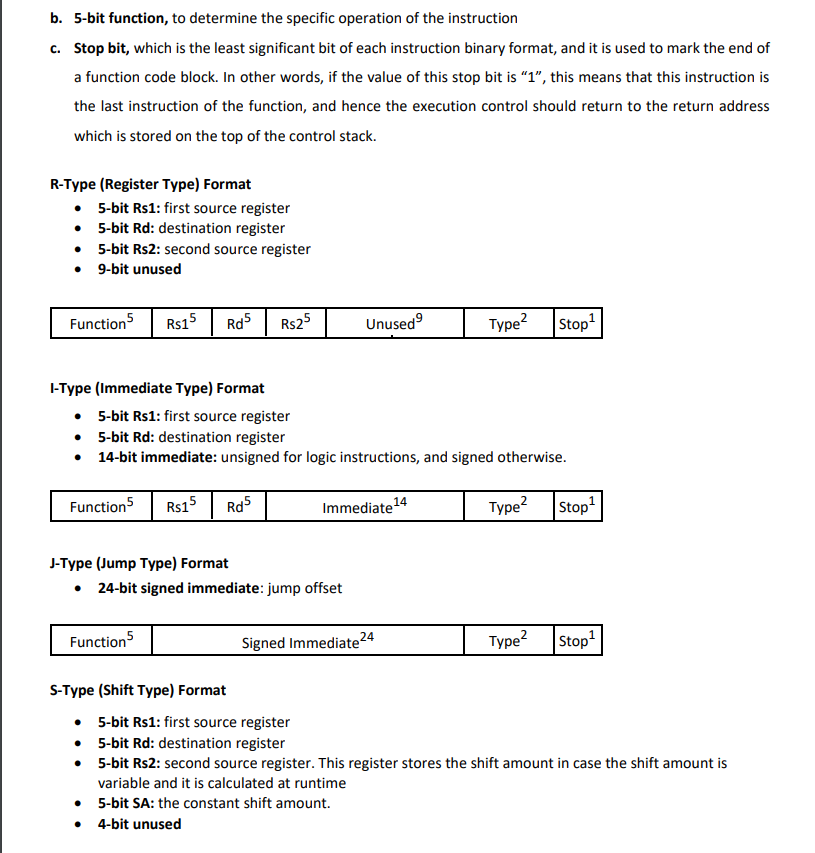
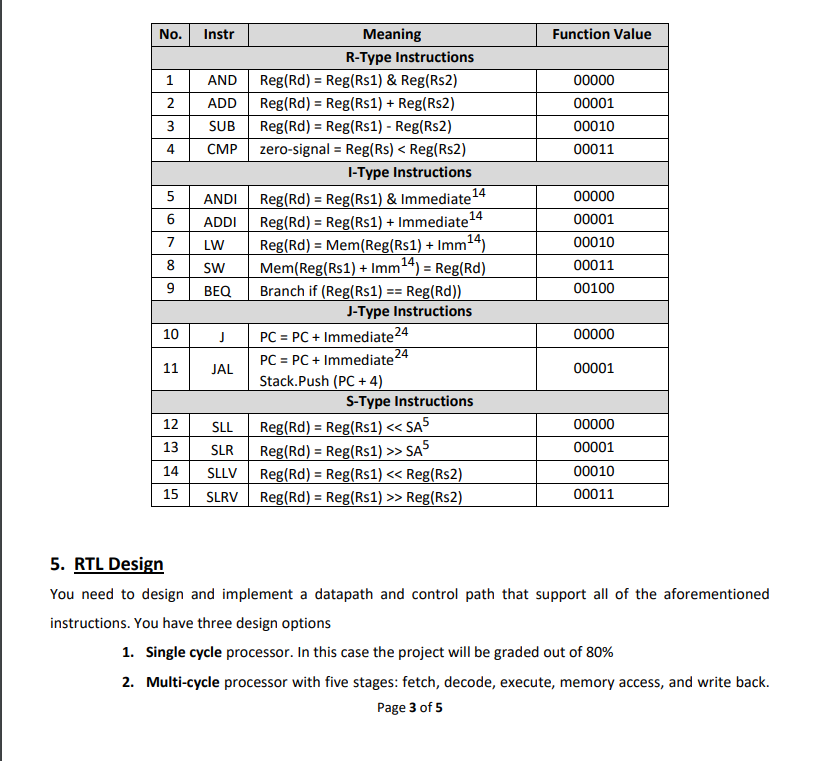
1. Objectives: To design and verify a simple RISC processor in Verilog 2. Processor Specifications 1. The instruction size is 32 bits 2. 32 32-bit general-purpose registers: from RO to R31. 3. A special purpose register for the program counter (PC) 4. It has a stack called control stack which saves the return addresses 5. Stack pointer (SP), another special purpose register to point to the top of the control stack. SP holds the address of the empty element on the top of the stack. For simplicity, you can assume a separate on-chip memory for the stack, and the initial value of SP is zero. 6. Four instruction types (R-type, 1-type, J-type, and S-type). 7. The processor's ALU has an output signal called "zero" signal, which is asserted when the result of the last ALU operation is zero. 8. Separate data and instructions memories 3. Instruction Types and Formats As mentioned above, this ISA has four instruction formats, namely, R-type, I-type, J-type, and S-type. These four types have the following common fields: a. 2-bit instruction type (00: R-Type, 01: J-Type, 10: l-type, 11: S-type) Page 1 of 5 b. 5-bit function, to determine the specific operation of the instruction c. Stop bit, which is the least significant bit of each instruction binary format, and it is used to mark the end of a function code block. In other words, if the value of this stop bit is "1", this means that this instruction is the last instruction of the function, and hence the execution control should return to the return address which is stored on the top of the control stack. R-Type (Register Type) Format 5-bit Rs1: first source register 5-bit Rd: destination register 5-bit Rs2: second source register 9-bit unused Function 5 I-Type (Immediate Type) Format Function5 Rs15 Rd5 Rs15 Rd5 Rs25 5-bit Rs1: first source register 5-bit Rd: destination register 14-bit immediate: unsigned for logic instructions, and signed otherwise. Function5 J-Type (Jump Type) Format 24-bit signed immediate: jump offset S-Type (Shift Type) Format Unused Immediate 4 14 Type Signed Immediate24 Type Stop Type 5-bit Rs1: first source register 5-bit Rd: destination register 5-bit Rs2: second source register. This register stores the shift amount in case the shift amount is variable and it is calculated at runtime 5-bit SA: the constant shift amount. 4-bit unused Stop Stop No. 1 2 3 4 5 6 7 8 9 10 11 12 13 14 15 Instr AND ADD SUB CMP ANDI ADDI LW SW BEQ J JAL SLL SLR SLLV SLRV Meaning R-Type Instructions Reg(Rd) = Reg(Rs1) & Reg(Rs2) Reg(Rd) = Reg(Rs1) + Reg(Rs2) Reg(Rd) = Reg(Rs1) - Reg(Rs2) zero-signal = Reg(Rs) < Reg(Rs2) I-Type Instructions Reg(Rd) = Reg(Rs1) & Immediate 4 Reg(Rd) Reg(Rs1) + Immediate 14 Reg(Rd) = Mem (Reg(Rs1) + Imm4) Mem(Reg(Rs1) +Imm4) Reg(Rd) Branch if (Reg(Rs1) == Reg(Rd)) J-Type Instructions 24 = PC = PC + Immediate24 PC = PC + Immediate24 Stack.Push (PC + 4) S-Type Instructions Reg(Rd) = Reg(Rs1) < < SA5 Reg(Rd) = Reg(Rs1) >> SA5 Reg(Rd) = Reg(Rs1) < < Reg(Rs2) Reg(Rd) = Reg(Rs1) >> Reg(Rs2) Function Value 00000 00001 00010 00011 00000 00001 00010 00011 00100 00000 00001 00000 00001 00010 00011 5. RTL Design You need to design and implement a datapath and control path that support all of the aforementioned instructions. You have three design options 1. Single cycle processor. In this case the project will be graded out of 80% 2. Multi-cycle processor with five stages: fetch, decode, execute, memory access, and write back. Page 3 of 5 In this case the project will be graded out of 100% 3. 5-stage pipelined processor (fetch, decode, execute, memory access, and write back). In this case, the project will be graded out of 120%, i.e., there is a bonus that can reach 20% of the project grade. 6. Verification To verify the RTL design, write a testbench around it. Moreover, you need to write multiple code sequences in the given ISA and show how the processor you designed executed these code sequences.
Step by Step Solution
3.51 Rating (144 Votes )
There are 3 Steps involved in it
The objectives of this project are to design and verify a simple RISC processor in Verilog The processor will have the following specifications The in... View full answer

Get step-by-step solutions from verified subject matter experts