

Question: 1. Simplify the following equations: b. X (M+N)(M+P) IN+P) 2. Draw the timing diagram for a digital signal that continuously alternates between 0.2 V(binary 0)
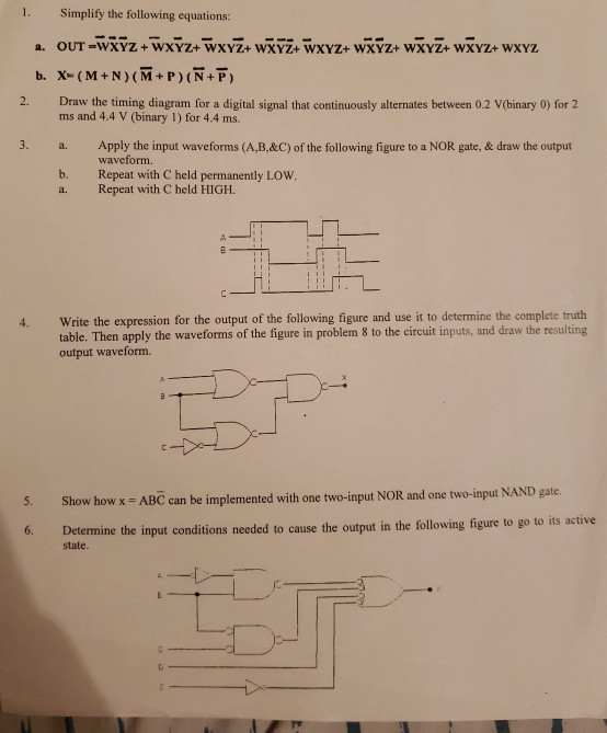
1. Simplify the following equations: b. X (M+N)(M+P) IN+P) 2. Draw the timing diagram for a digital signal that continuously alternates between 0.2 V(binary 0) for 2 ms and 4.4 V (binary 1) for 4.4 ms. a Apply the input waveforms (A,B,&C) of the following figure to a NOR gate, & draw the output b. Repeat with C held permanently LOW. 3. waveform a. Repeat with C held HIGH. Write the expression for the output of the following figure and use it to determine the complete truth table. Then apply the waveforms of the figure in problem 8 to the circuit inputs, and draw the resulting output waveform. 4. how how-ABC can be implemented with one two-input NOR and one two-input NAND gate. Determine the input conditions needed to cause the output in the following figure to go to its state. active 6
Step by Step Solution
There are 3 Steps involved in it

Get step-by-step solutions from verified subject matter experts