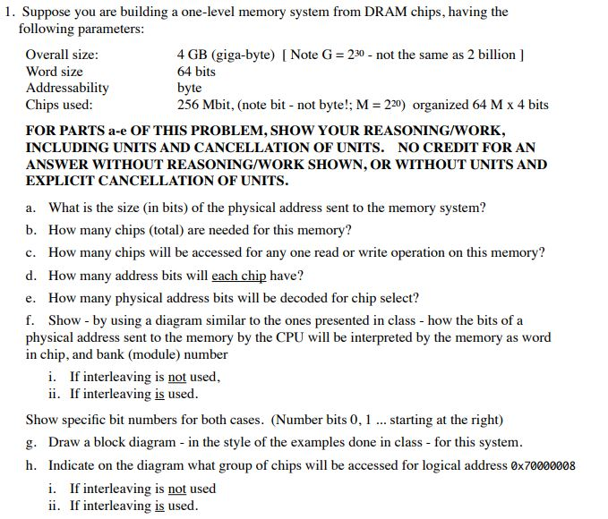
Question: 1. Suppose you are building a one-level memory system from DRAM chips, having the following parameters Overall size Word size Addressability Chips used FOR PARTS

1. Suppose you are building a one-level memory system from DRAM chips, having the following parameters Overall size Word size Addressability Chips used FOR PARTS a-e OF THIS PROBLEM, SHOW YOUR REASONING/WORK INCLUDING UNITS AND CANCELLATION OF UNITS. NO CREDIT FOR AN ANSWER WITHOUT REASONING/WORK SHOWN, OR WITHOUT UNITS AND EXPLICIT CANCELLATION OF UNITS 4 GB (giga-byte) [ Note G 230- not the same as 2 billion ] 64 bits byte 256 Mbit, (note bit-not byte!: M = 220) organized 64 M x 4 bits a. What is the size (in bits) of the physical address sent to the memory system? b. How many chips (total) are needed for this memory? c. How many chips will be accessed for any one read or write operation on this memory? d. How many address bits will each chip have? e. How many physical address bits will be decoded for chip select? f. Show - by using a diagram similar to the ones presented in class how the bits of a physical address sent to the memory by the CPU will be interpreted by the memory as word in chip, and bank (module) number i. If interleaving is not us ii. If interleaving is used Show specific bit numbers for both cases. (Number bits 0,1 .. starting at the right) g. Draw a block diagram in the style of the examples done in class for this system h. Indicate on the diagram what group of chips will be accessed for logical address 0x70000008 1. If interleaving is not used ii. If interleaving is used 1. Suppose you are building a one-level memory system from DRAM chips, having the following parameters Overall size Word size Addressability Chips used FOR PARTS a-e OF THIS PROBLEM, SHOW YOUR REASONING/WORK INCLUDING UNITS AND CANCELLATION OF UNITS. NO CREDIT FOR AN ANSWER WITHOUT REASONING/WORK SHOWN, OR WITHOUT UNITS AND EXPLICIT CANCELLATION OF UNITS 4 GB (giga-byte) [ Note G 230- not the same as 2 billion ] 64 bits byte 256 Mbit, (note bit-not byte!: M = 220) organized 64 M x 4 bits a. What is the size (in bits) of the physical address sent to the memory system? b. How many chips (total) are needed for this memory? c. How many chips will be accessed for any one read or write operation on this memory? d. How many address bits will each chip have? e. How many physical address bits will be decoded for chip select? f. Show - by using a diagram similar to the ones presented in class how the bits of a physical address sent to the memory by the CPU will be interpreted by the memory as word in chip, and bank (module) number i. If interleaving is not us ii. If interleaving is used Show specific bit numbers for both cases. (Number bits 0,1 .. starting at the right) g. Draw a block diagram in the style of the examples done in class for this system h. Indicate on the diagram what group of chips will be accessed for logical address 0x70000008 1. If interleaving is not used ii. If interleaving is used
Step by Step Solution
There are 3 Steps involved in it

Get step-by-step solutions from verified subject matter experts


