Question: please focus on these 3 questions and answer them based on the reading screenshots, do not use any outside sources. DO NOT USE ONLINE SOURCES,
please focus on these 3 questions and answer them based on the reading screenshots, do not use any outside sources.
DO NOT USE ONLINE SOURCES, DO NOT COPY?PASTE FROM ONLINE SOURCES.
ANSWER MUST BE BASED ON THE READING PROVIDED!!!!
1. Does Samsung have a cost advantage, a differentiation advantage, or both a cost and differentiation advantage over its rivals?
2: What are the resources and capabilities that form the basis of Samsungs cost or differentiation advantage(s)?
3. How difficult is it for competitors to replicate these resources and capabilities and thus how sustainable are Samsungs competitive advantage(s)
1-3 are the questions and this is all I know about the questions
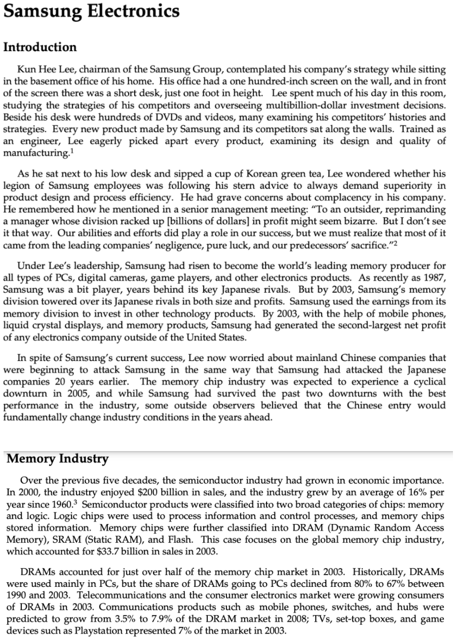
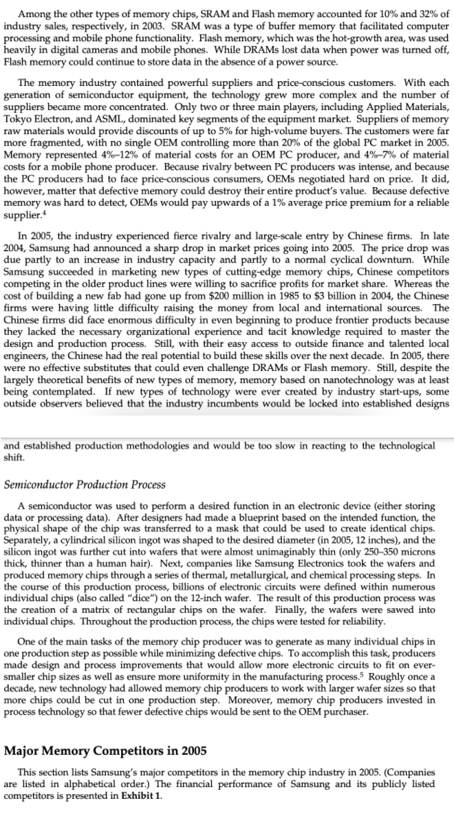
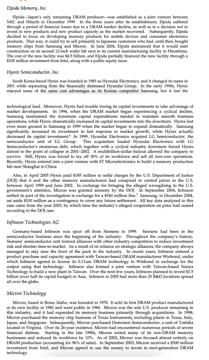
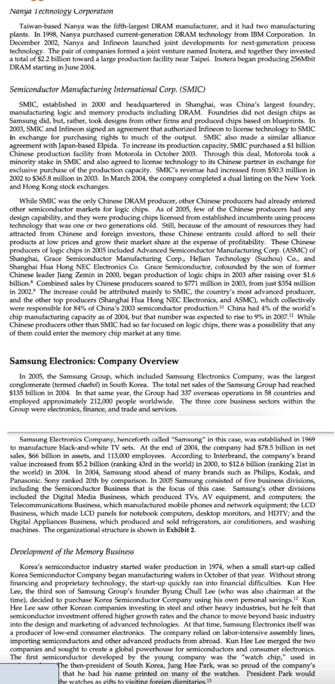
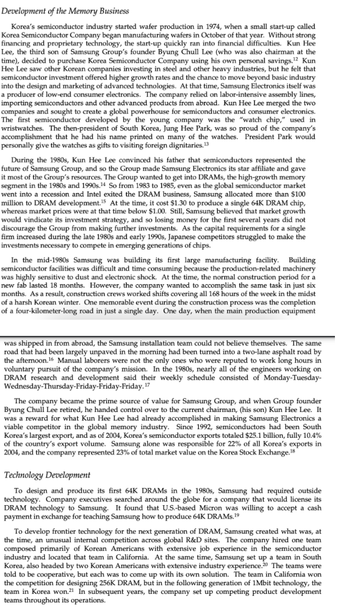
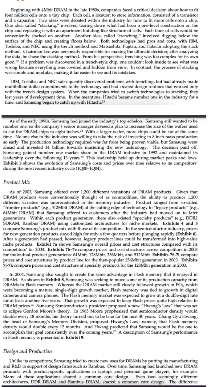
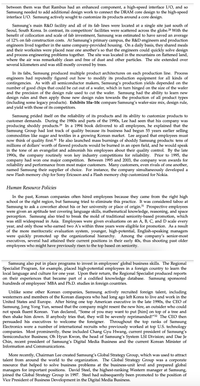
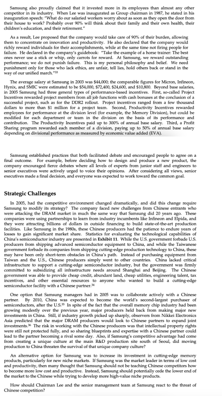
Samsung Electronics Introduction Kun Hee Lee, chairman of the Samsung Group, contemplated his company's strategy while sitting in the basement office of his home. His office had a one hundred-inch screen on the wall, and in front of the screen there was a short desk, just one foot in height. Lee spent much of his day in this room, studying the strategies of his competitors and overseeing multibillion-dollar investment decisions. Beside his desk were hundreds of DVDs and videos, many examining his competitors' histories and strategies. Every new product made by Samsung and its competitors sat along the walls. Trained as an engineer, Lee eagerly picked apart every product, examining its design and quality of manufacturing. As he sat next to his low desk and sipped a cup of Korean green tea, Lee wondered whether his legion of Samsung employees was following his stern advice to always demand superiority in product design and process efficiency. He had grave concerns about complacency in his company. He remembered how he mentioned in a senior management meeting: To an outsider, reprimanding a manager whose division racked up [billions of dollars] in profit might seem bizarre. But I don't see it that way. Our abilities and efforts did play a role in our success, but we must realize that most of it came from the leading companies' negligence, pure luck, and our predecessors' sacrifice." Under Lee's leadership, Samsung had risen to become the world's leading memory producer for all types of PCs, digital cameras, game players, and other electronics products. As recently as 1987, Samsung was a bit player, years behind its key Japanese rivals. But by 2003, Samsung's memory division towered over its Japanese rivals in both size and profits. Samsung used the earnings from its memory division to invest in other technology products. By 2003, with the help of mobile phones, liquid crystal displays, and memory products, Samsung had generated the second-largest net profit of any electronics company outside of the United States. In spite of Samsung's current success, Lee now worried about mainland Chinese companies that were beginning to attack Samsung in the same way that Samsung had attacked the Japanese companies 20 years earlier. The memory chip industry was expected to experience a cyclical downturn in 2005, and while Samsung had survived the past two downturns with the best performance in the industry, some outside observers believed that the Chinese entry would fundamentally change industry conditions in the years ahead. Memory Industry Over the previous five decades, the semiconductor industry had grown in economic importance. In 2000, the industry enjoyed $200 billion in sales, and the industry grew by an average of 16% per year since 1960. Semiconductor products were classified into two broad categories of chips: memory and logic. Logic chips were used to process information and control processes, and memory chips stored information. Memory chips were further classified into DRAM (Dynamic Random Access Memory), SRAM (Static RAM), and Flash. This case focuses on the global memory chip industry, which accounted for $33.7 billion in sales in 2003. DRAMs accounted for just over half of the memory chip market in 2003. Historically, DRAMS were used mainly in PCs, but the share of DRAMs going to PCs declined from 80% to 67% between 1990 and 2003. Telecommunications and the consumer electronics market were growing consumers of DRAMs in 2003. Communications products such as mobile phones, switches, and hubs were predicted to grow from 3.5% to 7.9% of the DRAM market in 2008; TVs, set-top boxes, and game devices such as Playstation represented 7% of the market in 2003. Among the other types of memory chips, SRAM and Flash memory accounted for 10% and 32% of industry sales, respectively, in 2003. SRAM was a type of buffer memory that facilitated computer processing and mobile phone functionality. Flash memory, which was the hot-growth area, was used heavily in digital cameras and mobile phones. While DRAMs lost data when power was turned off, Flash memory could continue to store data in the absence of a power source. The memory industry contained powerful suppliers and price-conscious customers. With each generation of semiconductor equipment, the technology grew more complex and the number of suppliers became more concentrated. Only two or three main players, including Applied Materials, Tokyo Electron, and ASML, dominated key segments of the equipment market. Suppliers of memory raw materials would provide discounts of up to 5% for high-volume buyers. The customers were far more fragmented, with no single OEM controlling more than 20% of the global PC market in 2005. Memory represented 4%-12% of material costs for an OEM PC producer, and 4%-7% of material costs for a mobile phone producer. Because rivalry between PC producers was intense, and because the PC producers had to face price-conscious consumers, OEMs negotiated hard on price. It did, however, matter that defective memory could destroy their entire product's value. Because defective memory was hard to detect, OEMs would pay upwards of a 1% average price premium for a reliable supplier. In 2005, the industry experienced fierce rivalry and large-scale entry by Chinese firms. In late 2004, Samsung had announced a sharp drop in market prices going into 2005. The price drop was due partly to an increase in industry capacity and partly to a normal cyclical downturn. While Samsung succeeded in marketing new types of cutting-edge memory chips, Chinese competitors competing in the older product lines were willing to sacrifice profits for market share. Whereas the cost of building a new fab had gone up from $200 million in 1985 to $3 billion in 2004, the Chinese firms were having little difficulty raising the money from local and international sources. The Chinese firms did face enormous difficulty in even beginning to produce frontier products because they lacked the necessary organizational experience and tacit knowledge required to master the design and production process. Still, with their easy access to outside finance and talented local engineers, the Chinese had the real potential to build these skills over the next decade. In 2005, there were no effective substitutes that could even challenge DRAMs or Flash memory. Still, despite the largely theoretical benefits of new types of memory, memory based on nanotechnology was at least being contemplated. If new types of technology were ever created by industry start-ups, some outside observers believed that the industry incumbents would be locked into established designs and established production methodologies and would be too slow in reacting to the technological shift. Semiconductor Production Process A semiconductor was used to perform a desired function in an electronic device (either storing data or processing data). After designers had made a blueprint based on the intended function, the physical shape of the chip was transferred to a mask that could be used to create identical chips. Separately, a cylindrical silicon ingot was shaped to the desired diameter (in 2005, 12 inches), and the silicon ingot was further cut into wafers that were almost unimaginably thin (only 250-350 microns thick, thinner than a human hair). Next, companies like Samsung Electronics took the wafers and produced memory chips through a series of thermal, metallurgical, and chemical processing steps. In the course of this production process, billions of electronic circuits were defined within numerous individual chips (also called "dice") on the 12-inch wafer. The result of this production process was the creation of a matrix of rectangular chips on the wafer. Finally, wafers were sawed into individual chips. Throughout the production process, the chips were tested for reliability. One of the main tasks of the memory chip producer was to generate as many individual chips in one production step as possible while minimizing defective chips. To accomplish this task, producers made design and process improvements that would allow more electronic circuits to fit on ever- smaller chip sizes as well as ensure more uniformity in the manufacturing process. Roughly once a decade, new technology had allowed memory chip producers to work with larger wafer sizes so that more chips could be cut in one production step. Moreover, memory chip producers invested in process technology so that fewer defective chips would be sent to the OEM purchaser. Major Memory Competitors in 2005 This section lists Samsung's major competitors in the memory chip industry in 2005. (Companies are listed in alphabetical order.) The financial performance of Samsung and its publicly listed competitors is presented in Exhibit 1. Elpida Memory, Inc. ElpidaJapan's only remaining DRAM producerwas established as a joint venture between NEC and Hitachi in December 1999. In the three years after its establishment, Elpida suffered through a period of financial losses due to a DRAM market decline, as well as to a decision not to invest in new products and new product capacity as the market recovered. Subsequently, Elpida decided to focus on developing memory products for mobile devices and consumer electronics products. That way, it could try to sell primarily to Japanese customers who had, until then, bought memory chips from Samsung and Micron. In June 2004, Elpida announced that it would start construction on its second 12-inch wafer fab next to its current manufacturing facility in Hiroshima. The cost of the new facility was $4.5 billion, and Elpida partially financed the new facility through a $100 million investment from Intel, along with a public equity issue. Hynix Semiconductor, Inc. South Korea-based Hynix was founded in 1983 as Hyundai Electronics, and it changed its name in 2001 while separating from the financially distressed Hyundai Group. In the early 1990s, Hynix enjoyed some of the same cost advantages as its Korean competitor Samsung, but it lost the technological lead. Moreover, Hynix had trouble timing its capital investments to take advantage of market developments. In 1996, when the DRAM market began experiencing a cyclical decline, Samsung maintained the minimum capital expenditures needed to maintain smooth business operations, while Hynix dramatically increased its capital investments into the downturn. Hynix lost even more ground to Samsung in 1999 when the market began to expand dramatically. Samsung significantly increased its investment in fast response to market growth, while Hynix actually decreased its capital investment. In 1999, Hyundai Electronics acquired LG Semiconductor, the semiconductor unit of LG Group. This acquisition loaded Hyundai Electronics with LG Semiconductor's enormous debt, which together with a cyclical industry downturn forced Hynix almost to the point of collapse in 20012002. A multibillion-dollar bailout allowed the company to survive. Still, Hynix was forced to lay off 30% of its workforce and sell all non-core operations. Recently, Hynix entered into a joint venture with ST Microelectronics to build a memory production fab near Shanghai in China. Also, in April 2005 Hynix paid $185 million to settle charges by the U.S. Department of Justice (DOJ) that it and the other memory manufacturers had conspired to control prices in the U.S. between April 1999 and June 2002. In exchange for bringing the alleged wrongdoing to the U.S. government's attention, Micron was granted amnesty by the DOJ. In September 2004, Infineon settled its part of the investigation in exchange for a $160 million fine.? Samsung, in December 2004, set aside $100 million as a contingency to cover any future settlement. All key data analyzed in this case came from the year 2003, by which time the industry's alleged cooperation on price had ceased according to the DOJ case. Infineon Technologies AG Germany-based Infineon was spun off from Siemens in 1999. Siemens had been in the semiconductor business since the beginning of the industry. Throughout the company's history, Siemens' semiconductor unit formed alliances with other industry competitors to reduce investment risk and shorten time-to-market. As a result of its reliance on strategic alliances, the company always managed to stay near the front of the pack in the industry. In recent years, Infineon entered a product purchase and capacity agreement with Taiwan-based DRAM manufacturer Winbond, under which Infineon agreed to license its 0.11um DRAM technology to Winbond in exchange for the output using that technology. Infineon also formed a joint venture with Taiwan-based Nanya Technology to build a new plant in Taiwan. Over the next few years, Infineon planned to invest $1.5 billion (over half its capital budget) in Asia. Infineon in 2005 had more than 25 R&D locations spread all over the globe. Micron Technology Micron, based in Boise, Idaho, was founded in 1978. It sold its first DRAM product manufactured at its own facility in 1982 and went public in 1984. Micron was the sole U.S. producer remaining in this industry, and it had expanded its memory business primarily through acquisitions. In 1998, Micron purchased the memory chip business of Texas Instruments, including plants in Texas, Italy, Japan, and Singapore. Subsequently, Micron purchased Dominion Semiconductor, a unit of Toshiba located in Virginia. Over its 26-year existence, Micron had encountered numerous periods of severe financial distress. Starting in the late 1990s, Micron exited many of its non-DRAM memory businesses and reduced its workforce by 10%. As of 2003, Micron was focused almost entirely on DRAM production (accounting for 96% of sales). In September 2003, Micron received a $500 million investment from Intel, and Micron agreed to use the money to invest in next-generation DRAM technology Nanya Technology Corporation Taiwan-based Nanya was the fifth-largest DRAM manufacturer, and it had two manufacturing plants. In 1998, Nanya purchased current-generation DRAM technology from IBM Corporation. In December 2002, Nanya and Infineon launched joint developments for next-generation process technology. The pair of companies formed a joint venture named Inotera, and together they invested a total of $2.2 billion toward a large production facility near Taipei. Inotera began producing 256Mbit DRAM starting in June 2004. Semiconductor Manufacturing International Corp. (SMIC) SMIC, established in 2000 and headquartered in Shanghai, was China's largest foundry, manufacturing logic and memory products including DRAM. Foundries did not design chips as Samsung did, but, rather, took designs from other firms and produced chips based on blueprints. In 2003, SMIC and Infineon signed an agreement that authorized Infineon to license technology to SMIC in exchange for purchasing rights to much of the output. SMIC also made a similar alliance agreement with Japan-based Elpida. To increase its production capacity, SMIC purchased a $1 billion Chinese production facility from Motorola in October 2003. Through this deal, Motorola took a minority stake in SMIC and also agreed to license technology to its Chinese partner in exchange for exclusive purchase of the production capacity. SMIC's revenue had increased from $50.3 million in 2002 to $365.8 million in 2003. In March 2004, the company completed a dual listing on the New York and Hong Kong stock exchanges. While SMIC was the only Chinese DRAM producer, other Chinese producers had already entered other semiconductor markets for logic chips. As of 2005, few of the Chinese producers had any design capability, and they were producing chips licensed from established incumbents using process technology that was one or two generations old. Still, because of the amount of resources they had attracted from Chinese and foreign investors, these Chinese entrants could afford to sell their products at low prices and grow their market share at the expense of profitability. These Chinese producers of logic chips in 2005 included Advanced Semiconductor Manufacturing Corp. (ASMC) of Shanghai, Grace Semiconductor Manufacturing Corp., Heian Technology (Suzhou) Co., and Shanghai Hua Hong NEC Electronics Co. Grace Semiconductor, cofounded by the son of former Chinese leader Jiang Zemin in 2000, began production of logic chips in 2003 after raising over $1.6 billion. Combined sales by Chinese producers soared to $771 million in 2003, from just $354 million in 2002. The increase could be attributed mainly to SMIC, the country's most advanced producer, and the other top producers (Shanghai Hua Hong NEC Electronics, and ASMC), which collectively were responsible for 84% of China's 2003 semiconductor production.10 China had 4% of the world's chip manufacturing capacity as of 2004, but that number was expected to rise to 9% in 2007.11 While Chinese producers other than SMIC had so far focused on logic chips, there was a possibility that any of them could enter the memory chip market at any time. Samsung Electronics: Company Overview In 2005, the Samsung Group, which included Samsung Electronics Company, was the largest conglomerate (termed chaebol) in South Korea. The total net sales of the Samsung Group had reached $135 billion in 2004. In that same year, the Group had 337 overseas operations in 58 countries and employed approximately 212,000 people worldwide. The three core business sectors within the Group were electronics, finance, and trade and services. Samsung Electronics Company, henceforth called "Samsung" in this case, was established in 1969 to manufacture black-and-white TV sets. At the end of 2004, the company had $78.5 billion in net sales, $66 billion in assets, and 113,000 employees. According to Interbrand, the company's brand value increased from $5.2 billion (ranking 43rd in the world) in 2000, to $12.6 billion (ranking 21st in the world) in 2004. In 2004, Samsung stood ahead of many brands such as Philips, Kodak, and Panasonic. Sony ranked 20th by comparison. In 2005 Samsung consisted of five business divisions, including the Semiconductor Business that is the focus of this case. Samsung's other divisions included the Digital Media Business, which produced TVs, AV equipment, and computers, the Telecommunications Business, which manufactured mobile phones and network equipment, the LCD Business, which made LCD panels for notebook computers, desktop monitors, and HDTV; and the Digital Appliances Business, which produced and sold refrigerators, conditioners, and washing machines. The organizational structure is shown in Exhibit 2. Development of the Memory Business Korea's semiconductor industry started wafer production in 1974, when a small start-up called Korea Semiconductor Company began manufacturing wafers in October of that year. Without strong financing and proprietary technology, the start-up quickly ran into financial difficulties. Kun Hee Lee, the third son of Samsung Group's founder Byung Chull Lee (who was also chairman at the time), decided to purchase Korea Semiconductor Company using his own personal savings.2 Kun Hee Lee saw other Korean companies investing in steel and other heavy industries, but he felt that semiconductor investment offered higher growth rates and the chance to move beyond basic industry into the design and marketing of advanced technologies. At that time, Samsung Electronics itself was a producer of low-end consumer electronics. The company relied on labor-intensive assembly lines, importing semiconductors and other advanced products from abroad. Kun Hee Lee merged the two companies and sought to create a global powerhouse for semiconductors and consumer electronics. The first semiconductor developed by the young company was the "watch chip, used in The then-president of South Korea, Jung Hee Park, was so proud of the company's that he had his name printed on many of the watches. President Park would the watches as gifts to visiting foreign dignitaries 13 Development of the Memory Business Korea's semiconductor industry started wafer production in 1974, when a small start-up called Korea Semiconductor Company began manufacturing wafers in October of that year. Without strong financing and proprietary technology, the start-up quickly ran into financial difficulties. Kun Hee Lee, the third son of Samsung Group's founder Byung Chull Lee (who was also chairman at the time), decided to purchase Korea Semiconductor Company using his own personal savings.2 Kun Hee Lee saw other Korean companies investing steel and other heavy industries, but he felt that semiconductor investment offered higher growth rates and the chance to move beyond basic industry into the design and marketing of advanced technologies. At that time, Samsung Electronics itself was a producer of low-end consumer electronics. The company relied on labor-intensive assembly lines, importing semiconductors and other advanced products from abroad. Kun Hee Lee merged the two companies and sought to create a global powerhouse for semiconductors and consumer electronics. The first semiconductor developed by the young company was the "watch chip, used in wristwatches. The then-president of South Korea, Jung Hee Park, was so proud of the company's accomplishment that he had his name printed on many of the watches. President Park would personally give the watches as gifts to visiting foreign dignitaries. 13 During the 1980s, Kun Hee Lee convinced his father that semiconductors represented the future of Samsung Group, and so the Group made Samsung Electronics its star affiliate and gave it most of the Group's resources. The Group wanted to get into DRAMs, the high-growth memory segment in the 1980s and 1990s.14 So from 1983 to 1985, even as the global semiconductor market went into a recession and Intel exited the DRAM business, Samsung allocated more than $100 million to DRAM development.15 At the time, it cost $1.30 to produce a single 64K DRAM chip, whereas market prices were at that time below $1.00. Still, Samsung believed that market growth would vindicate its investment strategy, and so losing money for the first several years did not discourage the Group from making further investments. As the capital requirements for a single firm increased during the late 1980s and early 1990s, Japanese competitors struggled to make the investments necessary to compete in emerging generations of chips. In the mid-1980s Samsung was building its first large manufacturing facility. Building semiconductor facilities was difficult and time consuming because the production-related machinery was highly sensitive to dust and electronic shock. At the time, the normal construction period for a new fab lasted 18 months. However, the company wanted to accomplish the same task in just six months. As a result, construction crews worked shifts covering all 168 hours of the week in the midst of a harsh Korean winter. One memorable event during the construction process was the completion of a four-kilometer-long road in just a single day. One day, when the main production equipment was shipped in from abroad, the Samsung installation team could not believe themselves. The same road that had been largely unpaved in the morning had been turned into a two-lane asphalt road by the afternoon. 16 Manual laborers were not the only ones who were reputed to work long hours in voluntary pursuit of the company's mission. In the 1980s, nearly all of the engineers working on DRAM research and development said their weekly schedule consisted of Monday Tuesday- Wednesday-Thursday-Friday-Friday-Friday. 17 The company became the prime source of value for Samsung Group, and when Group founder Byung Chull Lee retired, he handed control over to the current chairman, (his son) Kun Hee Lee. It was a reward for what Kun Hee Lee had already accomplished in making Samsung Electronics a viable competitor in the global memory industry. Since 1992, semiconductors had been South Korea's largest export, and as of 2004, Korea's semiconductor exports totaled $25.1 billion, fully 10.4% of the country's export volume. Samsung alone was responsible for 22% of all Korea's exports in 2004, and the company represented 23% of total market value on the Korea Stock Exchange 18 Technology Development To design and produce its first 64K DRAMs in the 1980s, Samsung had required outside technology. Company executives searched around the globe for a company that would license its DRAM technology to Samsung. It found that U.S.-based Micron was willing to accept a cash payment in exchange for teaching Samsung how to produce 64K DRAMs.19 To develop frontier technology for the next generation of DRAM, Samsung created what was, at the time, an unusual internal competition across global R&D sites. The company hired one team composed primarily of Korean Americans with extensive job experience in the semiconductor industry and located that team in California. At the same time, Samsung set up a team in South Korea, also headed by two Korean Americans with extensive industry experience.20 The teams were told to be cooperative, but each was to come up with its own solution. The team in California won the competition for designing 256K DRAM, but in the following generation of 1Mbit technology, the team in Korea won.21 In subsequent years, the company set up competing product development teams throughout its operations. Beginning with 4Mbit DRAM in the late 1980s, companies faced a critical decision about how to fit four million cells onto a tiny chip. Each cell, a location to store information, consisted of a transistor and a capacitor. Two ideas were debated within the industry for how to fit more cells onto a chip. One idea, called "stacking," involved tearing down what had been a one-level construction on the chip and replacing it with an apartment building-like structure of cells. Each floor of cells would be conveniently stacked on another. Another idea, called "trenching." involved digging below the surface of the chip and creating floors below. Both technologies had pros and cons, with IBM, Toshiba, and NEC using the trench method and Matsushita, Fujitsu, and Hitachi adopting the stack method. Chairman Lee was personally responsible for making the ultimate decision; after analyzing the data, he chose the stacking method. From his perspective, trenching was too complex for its own good.22 If a problem was discovered in a trench-style chip, one couldn't look inside to see what was wrong because everything was covered and hidden from view. In contrast, the process of stacking was simple and modular, making it far easier to see and fix mistakes. IBM, Toshiba, and NEC subsequently discovered problems with trenching, but had already made multibillion-dollar commitments to the technology and had created design routines that worked only with the trench design system. When the companies tried to switch technologies to stacking, they lost years of development time. In the meantime, Hitachi became number one in the industry for a time, and Samsung began to catch up with Hitachi.23 As of the early 1990s, Samsung had joined the industry's top echelon. Samsung still wanted to be number one, so the company's senior manager devised a plan to increase the size of the wafers used to cut the DRAM chips to eight inches.24 With a larger wafer, more chips could be cut at the same time. No one else in the industry was willing to take the risk of investing in 8-inch mass production so early. The production technology required was far from being proven viable, but Samsung went ahead and invested $1 billion towards mastering the new technology. The decision paid off. Samsung gained number one market share in the DRAM industry in 1992 and maintained its leadership over the following 13 years.25 This leadership held up during market peaks and lows. Exhibit 3 shows the evolution of Samsung's costs and prices over time relative to its competitors' during the most recent industry cycle (1000-1904). Product Mix As of 2003, Samsung offered over 1,200 different variations of DRAM products. Given that DRAM products were conventionally thought of as commodities, the ability to produce 1,200 different varieties was unprecedented in the memory industry. Product ranged from so-called "frontier products" (e.g., 512Mbit DRAM) at the cutting edge of technology to "legacy products" (e.g., 64Mbit DRAM) that Samsung offered to customers after the industry had moved on to later generations. Within each product generation, there also existed "specialty products" (eg., DDR2 SDRAM, Rambus DRAM) using customized architectures for niche markets. Exhibits 4 and 5 compare Samsung's product mix with those of its competitors. In the semiconductor industry, prices for new-generation products stayed high for only a few quarters before plunging rapidly (Exhibit 6). After a generation had passed, however, legacy product lines could be transformed into high-value niche products. Exhibit 7a shows Samsung's overall prices and cost structures compared with its competitors' for 2003. Exhibits 75-7e compare prices and cost structures across competitors in 2003 for individual product generations: 64Mbit, 128Mbit, 256Mbit, and 512Mbit. Exhibits 77-7i compare prices and cost structures by product line for the then-popular 256Mbit generation in 2003. Exhibits 71-7k compare prices and cost structure of specialty products for the 128Mbit generation in 2003. In 2004, Samsung also sought to create the same advantage in Flash memory that it enjoyed in DRAM. As shown in Exhibit 8, Samsung was seeking to move some of its production capacity from DRAMs to Flash memory. Whereas the DRAM market still closely followed growth in PCs, which were becoming a mature, single-digit growth market, Flash memory was tied to growth in digital cameras and camera phones. The Flash memory market was expected to grow at a double-digit rate for at least another five years. That growth was expected to keep Flash prices quite high relative to DRAM prices.26 Samsung Semiconductor's president proposed a new "Hwang's Law that was set to eclipse Gordon Moore's theory. In 1965 Moore prophesized that semiconductor density would double every 18 months; his theory turned out to be true for the next 40 years. Chang Gyu Hwang, the head of Samsung's Memory Division, proposed Hwang's Law, namely, that Flash memory density would double every 12 months. And Hwang predicted that Samsung would be the one to accomplish that goal consistently over the coming years.27 A description of Samsung's performance in Flash memory is presented in Exhibit 9. Design and Production Unlike its competitors, Samsung tried to create new uses for DRAMs by putting its manufacturing and R&D in support of design firms such as Rambus. Over time, Samsung had launched new DRAM products with product-specific applications in laptops and personal game players, for example. Many of these applications shared a common core design. Even two seemingly different architectures, DDR DRAM and Rambus DRAM, shared a common core design. The difference between them was that Rambus had an enhanced component, a high-speed interface I/O, and so Samsung needed to add additional design work to connect the DRAM core design to the high-speed interface I/O. Samsung actively sought to customize its products around a core design. Samsung's main R&D facility and all of its fab lines were located at a single site just south of Seoul, South Korea. In contrast, its competitors' facilities were scattered across the globe.28 With the benefit of collocation and scale of fab investment, Samsung was estimated to have saved an average of 12% on fab construction costs. At Samsung's primary campus, the R&D engineers and production engineers lived together in the same company provided housing. On a daily basis, they shared meals and their worksites were placed near one another's so that the engineers could quickly solve design and process engineering problems together. The site was located in the mountains on flattened land, where the air was remarkably clean and free of dust and other particles. The site extended over several kilometers and was still mostly covered by trees. In its fabs, Samsung produced multiple product architectures on each production line. Process engineers had reputedly figured out how to modify its production equipment for all kinds of contingencies. As with all semiconductor makers, Samsung's production yields depended on the number of good chips that could be cut out of a wafer, which in turn hinged on the size of the wafer and the precision of the design rule used to cut the wafer. Samsung had the ability to learn new design rules and then apply those new design rules towards the production of all product types (including some legacy products). Exhibits 102-10c compare Samsung's wafer-size mix, design rule, and yield with those of its competitors. Samsung prided itself on the reliability of its products and its ability to customize products to customer demands. During the 1980s and parts of the 1990s, Lee had seen that his company was producing shoddy products.29 In a 1994 book delivered to all employees, he explained that the Group had lost track of quality because its business had begun 55 years earlier selling now think of quality first.30 He also launched mass burnings of shoddy Samsung products: tens of millions of dollars' worth of flawed products would be burned in an open field, and he would speak in the tone of an evangelist and admonish his employees about their quality control. By the late 1990s, the company routinely won key industry competitions for reliability. Prior to 1995, the company had won one major competition. Between 1995 and 2003, the company won awards for reliability and performance from most major customers. Many customers, even rivals of one another, named Samsung their supplier of choice. For instance, the company simultaneously developed a new Flash memory chip for Sony Ericsson and a Flash memory chip customized for Nokia. . Human Resource Policies In the past, Korean companies often hired employees because they came from the right high school or the right region, but Samsung tried to eliminate this practice. It was considered taboo at Samsung to ask a coworker about his or her university or place of origin.31 Prospective employees were given an aptitude test covering language skills, mathematical knowledge, reasoning, and space perception. Samsung also tried to break the mold of traditional seniority-based promotion, which was still widespread in Asia. Employees were given evaluations on an A, B, C, and D scale every year, and only those who earned two A's within three years were eligible for promotion. As a result of the more meritocratic evaluation system, younger, high-potential, English-speaking managers were quickly promoted up the organizational hierarchy. Among the company's senior-most executives, several had attained their current positions in their early 40s, thus shooting past older employees who might have previously risen to the top based on seniority. Samsung also put in place programs to invest in employees' global business skills. The Regional Specialist Program, for example, placed high-potential employees in a foreign country to learn the local language and culture for one year. Upon their return, the Regional Specialist produced reports on their experiences that became part of a codified knowledge database. Samsung sponsored hundreds of employees' MBA and Ph.D. studies in foreign countries. Unlike some other Korean companies, Samsung actively recruited foreign talent, including westerners and members of the Korean diaspora who had long ago left Korea to live and work in the United States and Europe. After hiring one top American executive in the late 1990s, the CEO of Samsung, Jong Yong Yun, sensed that the company might resent the new hire, an outsider who could not speak fluent Korean. Yun declared, "Some of you may want to put [him) on top of a tree and then shake him down. If anybody tries that, they will be severely reprimanded!"32 The CEO then persuaded his executives to welcome the foreigner. Throughout the top ranks of Samsung Electronics were a number of international recruits who previously worked at top U.S. technology companies. Most prominently, these included Chang Gyu Hwang, current president of Samsung's Semiconductor Business; Oh Hyun Kwon, the head of Samsung's System LSI Division, and Dae Je Chin, recent president of Samsung's Digital Media Business and the current Korean Minister of Information and Communications. More recently, Chairman Lee created Samsung's Global Strategy Group, which was used to attract talent from around the world to the organization. The Global Strategy Group was a corporate resource that helped to solve business problems at the business-unit level and prepared global managers for important positions. David Steel, the highest-ranking Western manager at Samsung, joined the Global Strategy Group in 1997. Steel had subsequently been promoted to the position of Vice President of Business Development in the Digital Media Business. Samsung also proudly claimed that it invested more in its employees than almost any other competitor in its industry. When Lee was inaugurated as Group chairman in 1987, he stated in his inauguration speech: "What do our salaried workers worry about as soon as they open the door from their house to work? Probably over 90% will think about their family and their own health, their children's education, and their retirement." As a result, Lee proposed that the company would take care of 90% of their burden, allowing them to concentrate on innovation and productivity. He also declared that the company would richly reward individuals for their accomplishments, while at the same time not firing people for failure. He declared in the company's guidebook: "Take the example of a horse trainer: The best ones never use a stick or whip, only carrots for reward. At Samsung, we reward outstanding performance; we do not punish failure. This is my personal philosophy and belief. We need punishment only for those who lack ethics, are unfair, tell lies, hold others back or stand in the way of our unified march."33 The average salary at Samsung in 2003 was $44,000; the comparable figures for Micron, Infineon, Hynix, and SMIC were estimated to be $54,000, $72,400, $24,600, and $10,800. Beyond base salaries, in 2005 Samsung had three general types of performance-based incentives. First, so-called Project Incentives rewarded project members from all job functions with cash bonuses at the conclusion of a successful project, such for the DDR2 rollout. Project incentives ranged from a few thousand dollars to more than $1 million for a project team. Second, Productivity Incentives rewarded employees for performance at the division level (for example, the Memory Division), but could be modified for each department or team in the division on the basis of its performance and contribution. The Productivity Incentives paid up to 300% of annual base salary. Third, a Profit Sharing program rewarded each member of a division, paying up to 50% of annual base salary depending on divisional performance as measured by economic value added (EVA). Samsung established practices that both facilitated debate and encouraged people to agree on a final outcome. For example, before deciding how to design and produce a new product, the company encouraged fierce debates where all levels of experts from junior staff and engineers to senior executives were actively urged to voice their opinions. After considering all views, senior executives made a final decision, and everyone was expected to work toward the common goal. Strategic Challenges In 2005, had the competitive environment changed dramatically, and did this change require Samsung to modify its strategy? The company faced new challenges from Chinese entrants who were attacking the DRAM market in much the same way that Samsung did 20 years ago. These companies were using partnerships to learn from industry incumbents like Infineon and Elpida, and they were attracting billions of dollars in outside financing to build state-of-the-art production facilities. Like Samsung in the 1980s, these Chinese producers had the patience to endure years of losses to gain significant market share. Statistics for evaluating the technological capabilities of China's semiconductor industry are presented in Exhibit 11. While the U.S. government forbade U.S. producers from shipping advanced semiconductor equipment to China, and while the Taiwanese government forbade its companies from shipping cutting-edge production technology to China, these may have been only short-term obstacles in China's path. Instead of purchasing equipment from Taiwan and the U.S., Chinese producers simply went to other countries. China lacked critical infrastructure to support a cutting-edge semiconductor industry, but the government was firmly committed to subsidizing all infrastructure needs around Shanghai and Beijing. The Chinese government was able to provide cheap credit, abundant land, cheap utilities, engineering talent, tax incentives, and other essential resources to anyone who wanted to build a cutting-edge semiconductor facility with a Chinese partner.34 One option that Samsung managers had in 2005 was to collaborate actively with a Chinese partner. By 2010, China was expected to become the world's second-largest purchaser of semiconductors, after the U.S.35 In spite of the fact that the overall memory chip industry had been growing modestly over the previous year, major producers held back from making major new investments in China. Still, if industry growth picked up sharply, observers from Nikkei Electronics Asia predicted that the major DRAM producers would look to Chinese partners to expand joint investments.36 The risk in working with the Chinese producers was that intellectual property rights were still not protected fully, and so sharing blueprints and expertise with a Chinese partner could lead to the partner becoming a rival some day. Also, if Samsung's competitive advantage had come from creating a unique culture at the main R&D production site south of Seoul, did moving production to China threaten the survival of that unique company culture? An alternative option for Samsung was to increase its investment in cutting-edge memory products, particularly for new niche markets. If Samsung was the market leader in terms of low cost and productivity, then many thought that Samsung should not be teaching Chinese competitors how to become more low cost and productive. Instead, Samsung should potentially cede the lower end of the market to the Chinese while trying to develop more high-value niche products. How should Chairman Lee and the senior management team at Samsung react to the threat of Chinese competitionStep by Step Solution
There are 3 Steps involved in it

Get step-by-step solutions from verified subject matter experts


