

Question: 2. Design a circuit that implements function f below using AND, OR, and NOT gates. Do not attempt to change the form of the equation.
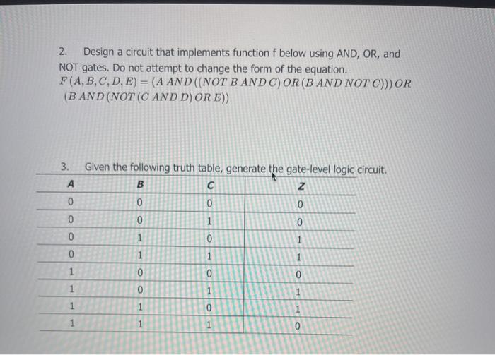

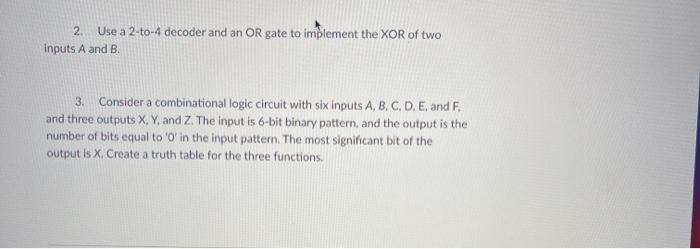
2. Design a circuit that implements function f below using AND, OR, and NOT gates. Do not attempt to change the form of the equation. F(A, B, C, D, E) = (A AND ((NOT B AND C) OR (BAND NOT C))) OR (BAND (NOT (CAND DOR E)) 3 . 3. Given the following truth table, generate the gate-level logic circuit. B C N 0 0 0 0 0 1 0 0 0 0 1 0 1 1 1 1 1 0 0 0 1 0 1 1 1 1 0 1 1 1 1 0 B. Combinational Circuits 1. Use a 4-to-1 MUX to implement each of the following functions. A B Y "O 0 0 1 0 1 1 0 1 0 1 O 1 1 1 0 1 2 Use a 2-to-4 decoder and an OR gate to implement the XOR of two inputs A and B. 3. Consider a combinational logic circuit with six inputs A, B, C, D, E, and F. and three outputs X, Y, and Z. The input is 6-bit binary pattern, and the output is the number of bits equal to 'O' in the input pattern. The most significant bit of the output is X. Create a truth table for the three functions
Step by Step Solution
There are 3 Steps involved in it

Get step-by-step solutions from verified subject matter experts