

Question: 2.) Objective The objective of this practical is to develop a code converter block that can be used to convert numeric and symbol characters that
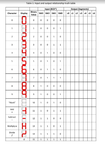
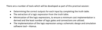
2.) Objective The objective of this practical is to develop a code converter block that can be used to convert numeric and symbol characters that were encoded using binary, to be displayed on a 7-segment display. The resulting code converter block should consist of the smallest possible number of logic gates and connections and must be simulated on Atanua using a 7- segment display and four switches SW3 (MSB), SW2, Swi and SWO (LSB). For this practical you are NOT allowed to use any 74-series chips to drive the 7-segment display. The input value and output segment relationships are displayed in the truth table provided in Table 1. Table 1: Input and output relationship truth table Input (BCD) Output (Sesments) Binary Display Value SW SW2 swi SWO 0 0 Character 0 o 1 0 0 1 2 0 0 1 0 3 1 1 0 1 0 0 JIQUOJUONTOO 0 O 1 2 1 0 0 0 D o "lank" 10 1 0 Add + 0 1 1 Subtract 12 0 0 Multiply 8 13 1 1 1 Divide 1 14 0 15 There are a number of tools which will be developed as part of this practical session Determining the correct outputs for each input by completing the truth table. The extraction of a logic expression from the truth table Minimization of the logic expressions, to ensure a minimum cost implementation is derived and the least number of logic gates and connections are utilized. The implementation of the logic expression using a schematic design and simulation software tool - Atanus. 2.) Objective The objective of this practical is to develop a code converter block that can be used to convert numeric and symbol characters that were encoded using binary, to be displayed on a 7-segment display. The resulting code converter block should consist of the smallest possible number of logic gates and connections and must be simulated on Atanua using a 7- segment display and four switches SW3 (MSB), SW2, Swi and SWO (LSB). For this practical you are NOT allowed to use any 74-series chips to drive the 7-segment display. The input value and output segment relationships are displayed in the truth table provided in Table 1. Table 1: Input and output relationship truth table Input (BCD) Output (Sesments) Binary Display Value SW SW2 swi SWO 0 0 Character 0 o 1 0 0 1 2 0 0 1 0 3 1 1 0 1 0 0 JIQUOJUONTOO 0 O 1 2 1 0 0 0 D o "lank" 10 1 0 Add + 0 1 1 Subtract 12 0 0 Multiply 8 13 1 1 1 Divide 1 14 0 15 There are a number of tools which will be developed as part of this practical session Determining the correct outputs for each input by completing the truth table. The extraction of a logic expression from the truth table Minimization of the logic expressions, to ensure a minimum cost implementation is derived and the least number of logic gates and connections are utilized. The implementation of the logic expression using a schematic design and simulation software tool - Atanus
Step by Step Solution
There are 3 Steps involved in it

Get step-by-step solutions from verified subject matter experts