

Question: 3. (12 marks) In this assignment you will design a multiply-divide hardware which can be used readily in a MIPS processor. In particular, we focus
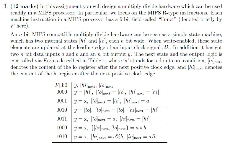
3. (12 marks) In this assignment you will design a multiply-divide hardware which can be used readily in a MIPS processor. In particular, we focus on the MIPS R-type instructions. Each machine instruction in a MIPS processor has a 6 bit field called "Funct (denoted briefly by F here) An n bit MIPS compatible multiply-divide hardware can be seen as a simple state machine, which has two internal states [hi and [lo, each n bit wide. When write-enabled, these state elements are updated at the leading edge of an input clock signal clk. In addition it has got two n bit data inputs a and b and an n bit output y. The next state and the output logic is controlled via F3o as described in Table 1, where 'x' stands for a don't care condition, [lonext denotes the content of the lo register after the next positive clock edge, and [hinext denotes the content of the hi register after the next positive clock edge 0001 | y=x, [10]next -llo, lhi)next-a 0011 | y = x, [10]next 1000 | y = x, 1010 | y=x. lhi]next0%b. [10]next-a/b =a, [hi]next[hi] hi lo next, o next } = a * b 3. (12 marks) In this assignment you will design a multiply-divide hardware which can be used readily in a MIPS processor. In particular, we focus on the MIPS R-type instructions. Each machine instruction in a MIPS processor has a 6 bit field called "Funct (denoted briefly by F here) An n bit MIPS compatible multiply-divide hardware can be seen as a simple state machine, which has two internal states [hi and [lo, each n bit wide. When write-enabled, these state elements are updated at the leading edge of an input clock signal clk. In addition it has got two n bit data inputs a and b and an n bit output y. The next state and the output logic is controlled via F3o as described in Table 1, where 'x' stands for a don't care condition, [lonext denotes the content of the lo register after the next positive clock edge, and [hinext denotes the content of the hi register after the next positive clock edge 0001 | y=x, [10]next -llo, lhi)next-a 0011 | y = x, [10]next 1000 | y = x, 1010 | y=x. lhi]next0%b. [10]next-a/b =a, [hi]next[hi] hi lo next, o next } = a * b
Step by Step Solution
There are 3 Steps involved in it

Get step-by-step solutions from verified subject matter experts