

Question: 3. (5 points) You are tasked with designing an 8 element micro-sensor array on a chip in a CMOS process. Because of space constraints on
3. (5 points) You are tasked with designing an 8 element micro-sensor array on a chip in a CMOS process. Because of space constraints on the silicon die, it is advantageous in minimizing area (chip pad count) to use a binary addressing system to activate each array element. This way, only 1 external input is applied for the row (R0), and 2 for the column (C0, C1) so that only 3 pads are required to address 8 elements. This particular array has 2 rows and 4 columns. Each of these elements is activated when both its row and column enable inputs are logic 1. Only one sensor is allowed to be active at once. Therefore, the array is configured as follows: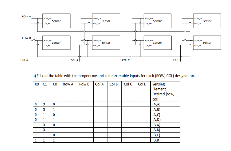
b) Draw the logic circuit that implements this system and show how it connects to the sensors, using two decoders. It may be helpful to rewrite the table from part (a) into the format below.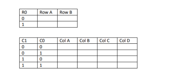
c) Why is the decoder implementation much more straightforward than a multiplexer implementation? You could show different multiplexer solutions to compare with your answer to part (b).
ROW A ROW EN ROW EN Sensor Sensor Sersor Sensor ROW B ROW EN ROW EN Sensor Sensor Sersor Sensor COLA COL B COL C COL D a) Fill out the table with the proper row and column enable inputs for each (ROW, COL) designation. RO C1 CO Row A Row B Col A Col B Col C Col DSensing Element Desired (row col A,A) A,B) 0 0 1 A,D) B,A B,B) B,C) B,D 0 1 1 110 RO 0 Row A Row B C1 CO Col A Col B Col C Col D 0 0 1 1 CD 0
Step by Step Solution
There are 3 Steps involved in it

Get step-by-step solutions from verified subject matter experts