

Question: 4. (25 points) Single Cycle Datapath. Given the following MIPS instruction sequence executed on a single cycle datapath (Note that little Endian is used). Fill
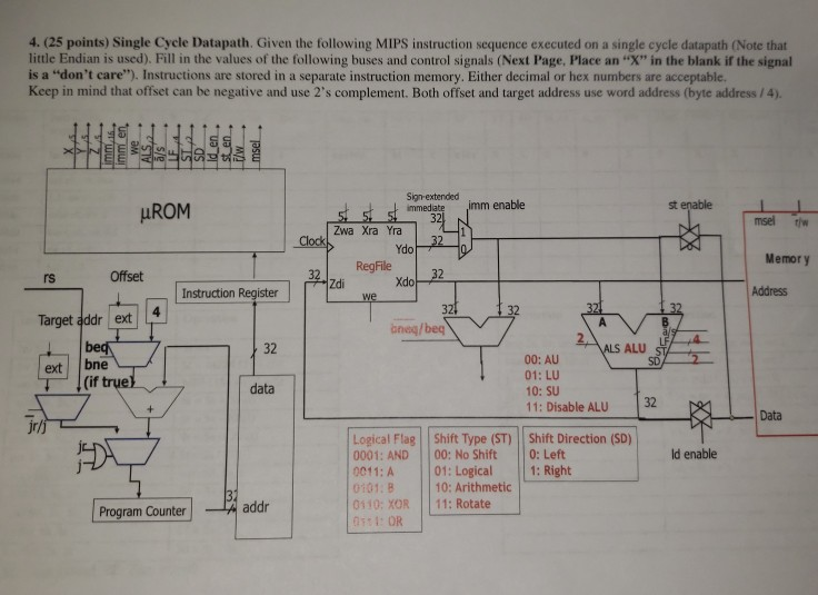
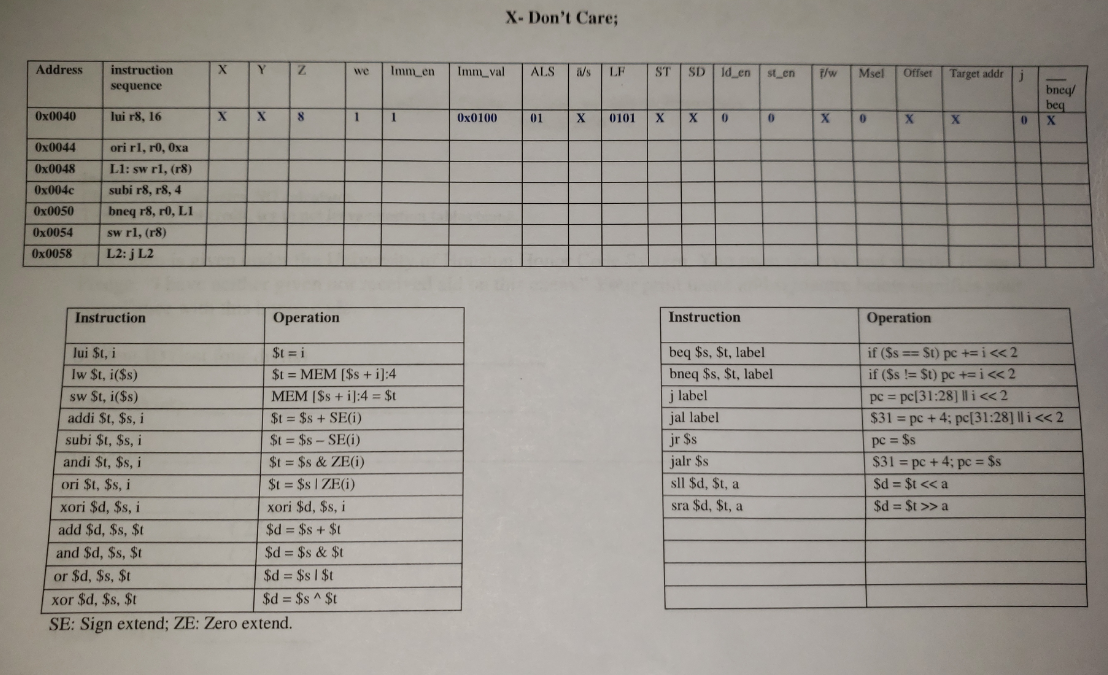
4. (25 points) Single Cycle Datapath. Given the following MIPS instruction sequence executed on a single cycle datapath (Note that little Endian is used). Fill in the values of the following buses and control signals (Next Page. Place an "X" in the blank if the signal is a "don't care"). Instructions are stored in a separate instruction memory. Either decimal or hex numbers are acceptable. Keep in mind that offset can be negative and use 2's complement. Both offset and target address use word address (byte address/4). imm 16. imm en id en sten F/W msel Sign-extended UROM st enable 5 51 st immediate imm enable mselt Clock 320 Zwa Xra Yra Ydo RegFile Xdo Regilea 22 Memory Offset 32. Zdi Instruction Register Address 32 132 Target addrext hned/beg ben 32 corte bne (if true} data 00: AU 01: LU 10: SU 11: Disable ALU Data Shift Direction (SD) || 0: Left 1: Right Id enable Logical Flag 0001: AND 0011: A 0101.B 0110: XOR 0101: OR Shift Type (ST) 00: No Shift 01: Logical 10: Arithmetic 11: Rotate Program Counter A addr X- Don't Care; Address instruction sequence we Imm_en we en sl_en /w Msel Offset Target addr Imm_val 0x0100 ALS W 01 LF ST | SD 0101 x x bney/ beg Ox0040 lui r8, 16 X X 0x0044 0x0048 0x0040 Ox0050 Ox0054 0x0058 ori rl, r, Oxa L1: sw rl, (r) subi r8, r8,4 bneq r8, ro, LI sw rl, (r8) L2:jL2 Instruction Operation Instruction Operation if ($s == St) pc +=i a 4. (25 points) Single Cycle Datapath. Given the following MIPS instruction sequence executed on a single cycle datapath (Note that little Endian is used). Fill in the values of the following buses and control signals (Next Page. Place an "X" in the blank if the signal is a "don't care"). Instructions are stored in a separate instruction memory. Either decimal or hex numbers are acceptable. Keep in mind that offset can be negative and use 2's complement. Both offset and target address use word address (byte address/4). imm 16. imm en id en sten F/W msel Sign-extended UROM st enable 5 51 st immediate imm enable mselt Clock 320 Zwa Xra Yra Ydo RegFile Xdo Regilea 22 Memory Offset 32. Zdi Instruction Register Address 32 132 Target addrext hned/beg ben 32 corte bne (if true} data 00: AU 01: LU 10: SU 11: Disable ALU Data Shift Direction (SD) || 0: Left 1: Right Id enable Logical Flag 0001: AND 0011: A 0101.B 0110: XOR 0101: OR Shift Type (ST) 00: No Shift 01: Logical 10: Arithmetic 11: Rotate Program Counter A addr X- Don't Care; Address instruction sequence we Imm_en we en sl_en /w Msel Offset Target addr Imm_val 0x0100 ALS W 01 LF ST | SD 0101 x x bney/ beg Ox0040 lui r8, 16 X X 0x0044 0x0048 0x0040 Ox0050 Ox0054 0x0058 ori rl, r, Oxa L1: sw rl, (r) subi r8, r8,4 bneq r8, ro, LI sw rl, (r8) L2:jL2 Instruction Operation Instruction Operation if ($s == St) pc +=i a
Step by Step Solution
There are 3 Steps involved in it

Get step-by-step solutions from verified subject matter experts