

Question: 4. The block diagram for a single cycle MIPS processor is shown in the figure below. And the latencies (time delay) of major blocks
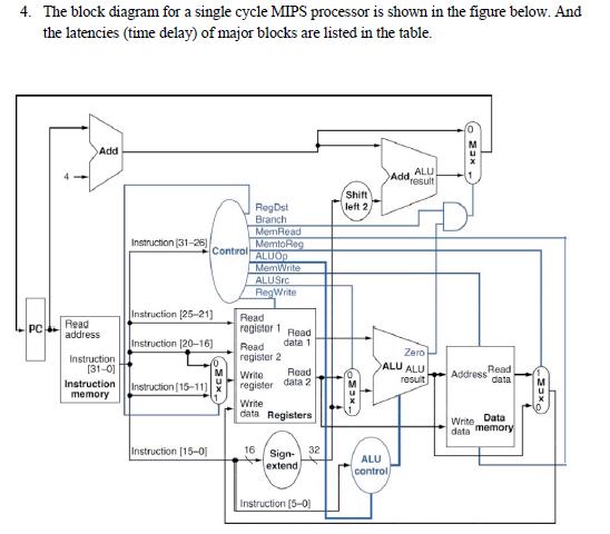
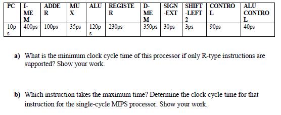
4. The block diagram for a single cycle MIPS processor is shown in the figure below. And the latencies (time delay) of major blocks are listed in the table. 4- Add (o Zax Add, ALU result RegDat Shift left 2, Branch MemRead Instruction (31-26)| MemtoReg Control ALUOD MemWrite ALUSIC RegWrite Instruction [25-21] Read PC Read address registor 1 Read Instruction [20-16] date 1 Instruction. [31-0] Read register 2 Zero Write Read ALU ALU Address Read Instruction data 2 result data Instruction[15-11)] register memory Write data Registers Write Data data memory Instruction [15-0 16 Sign- extend 32 ALU control Instruction (5-0) (-=0x) PC I- ME M ADDE R MU ALU REGISTE D- X R SIGN SHIFT CONTRO ME -EXT -LEFT L ALU CONTRO M 2 L 10p 400ps 100ps 35ps 120p 230ps 350ps 30ps 3ps 90ps 40ps S S a) What is the minimum clock cycle time of this processor if only R-type instructions are supported? Show your work. b) Which instruction takes the maximum time? Determine the clock cycle time for that instruction for the single-cycle MIPS processor. Show your work.
Step by Step Solution
There are 3 Steps involved in it

Get step-by-step solutions from verified subject matter experts