

Question: 6. For the following Verilog code, draw the corresponding circuit diagram for bigMod. Your circuit should only involve standard gates (AND, OR, NAND, NOR,
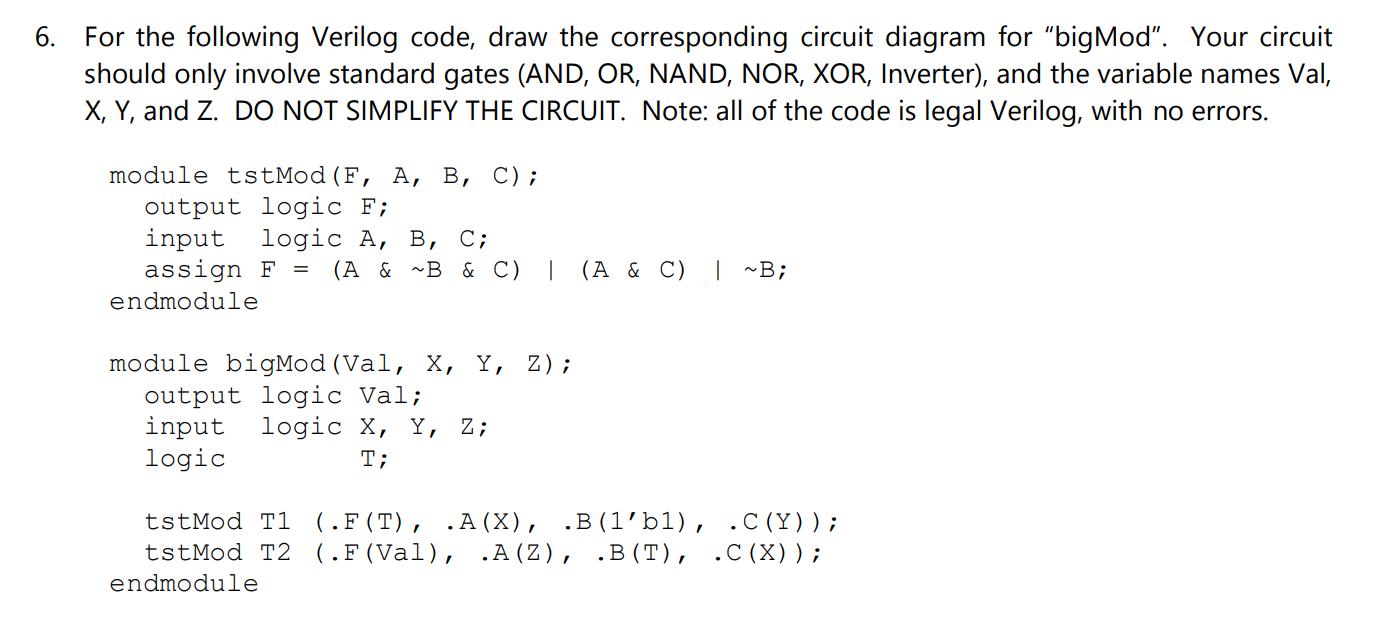
6. For the following Verilog code, draw the corresponding circuit diagram for "bigMod". Your circuit should only involve standard gates (AND, OR, NAND, NOR, XOR, Inverter), and the variable names Val, X, Y, and Z. DO NOT SIMPLIFY THE CIRCUIT. Note: all of the code is legal Verilog, with no errors. module tstMod (F, A, B, C); output logic F; input logic A, B, C; assign F (A & B & C) | (A & C) endmodule module bigMod (Val, X, Y, output logic Val; input logic X, Y, Z; logic T; Z); tstMod T1 (.F (T), .A (X), B (1'bl), tstMod T2 (.F (Val), .A (Z), .B(T), endmodule | ~B; .C (Y)); .C (X));
Step by Step Solution
There are 3 Steps involved in it
Answer To draw the corresponding circuit diagram for ... View full answer

Get step-by-step solutions from verified subject matter experts