

Question: a) b) M X M Consider the circuit shown in Figure B1 (a), assuming - L-2 = 1.0 m, W-2 = 2.0 m, L34
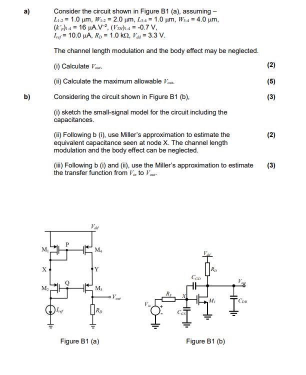
a) b) M X M Consider the circuit shown in Figure B1 (a), assuming - L-2 = 1.0 m, W-2 = 2.0 m, L34 = 1.0 m, W34 = 4.0 m, (kp)1-4 = 16 A.V-2, (VT)1-4 = -0.7 V, Tref= 10.0 A, RD=1.0 k, Vad = 3.3 V. The channel length modulation and the body effect may be neglected. (i) Calculate Vou (ii) Calculate the maximum allowable Vout- Considering the circuit shown in Figure B1 (b), (i) sketch the small-signal model for the circuit including the capacitances. (ii) Following b (i), use Miller's approximation to estimate the equivalent capacitance seen at node X. The channel length modulation and the body effect can be neglected. Ive (iii) Following b (i) and (ii), use the Miller's approximation to estimate (3) the transfer function from Vin to Vou Va M M R Figure B1 (a) V Rs CGD Ro M Figure B1 (b) (2) (5) (3) CDB (2)
Step by Step Solution
3.40 Rating (150 Votes )
There are 3 Steps involved in it
To calculate Vi and the maximum allowable Vout for the circuit in Figure B1a we need to examine the ... View full answer

Get step-by-step solutions from verified subject matter experts