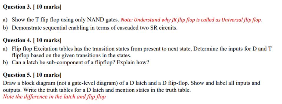
Question: a) Draw the complete circuit diagram for a SR-flip flop using only NAND gates. b) Provide the truth table for the circuit in part


a) Draw the complete circuit diagram for a SR-flip flop using only NAND gates. b) Provide the truth table for the circuit in part a) c) Which state in SR latch is not stable? Briefly explain the reason using a tracing diagram of SR latch for respective state. Question 2. [10 marks] a) Draw the complete circuit diagram for a JK flip flop, using fundamental logic gates. Label your diagram. b) Design and draw an equivalent circuit for a D-flip flop using only a JK-flip flop and NOR gate(s). Use a block diagram for the JK-flip flop. Question 3. [10 marks] a) Show the T flip flop using only NAND gates. Note: Understand why JK flip flop is called as Universal flip flop. b) Demonstrate sequential enabling in terms of cascaded two SR circuits. Question 4. [10 marks] a) Flip flop Excitation tables has the transition states from present to next state, Determine the inputs for D and T flipflop based on the given transitions in the states. b) Can a latch be sub-component of a flipflop? Explain how? Question 5. [10 marks] Draw a block diagram (not a gate-level diagram) of a D latch and a D flip-flop. Show and label all inputs and outputs. Write the truth tables for a D latch and mention states in the truth table. Note the difference in the latch and flip flop
Step by Step Solution
There are 3 Steps involved in it

Get step-by-step solutions from verified subject matter experts


