

Question: A Figure D2: A combinational circuit 4. Complete the truth table for the circuit in Figure D2 in Table F1 (Section F). 5. Convert the
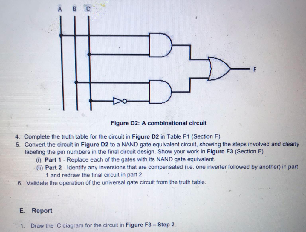
A Figure D2: A combinational circuit 4. Complete the truth table for the circuit in Figure D2 in Table F1 (Section F). 5. Convert the circuit in Figure D2 to a NAND gate equivalent circuit, showing the steps involved and clearly labeling the pin numbers in the final circuit design. Show your work in Figure F3 (Section F). (i) Part 1 - Replace each of the gates with its NAND gate equivalent. (ii) Part 2 - Identify any inversions that are compensated (i.e. one inverter followed by another) in part 1 and redraw the final circuit in part 2 6. Validate the operation of the universal gate circuit from the truth table. E. Report 1. Draw the IC diagram for the circuit in Figure F3 - Step 2
Step by Step Solution
There are 3 Steps involved in it

Get step-by-step solutions from verified subject matter experts