

Question: PLEASE DO PHASE 3 **URGENT** Problem statement: In this project, you will design and implement a Logic Unit using Quartus II design tools. The system
 PLEASE DO PHASE 3 **URGENT**
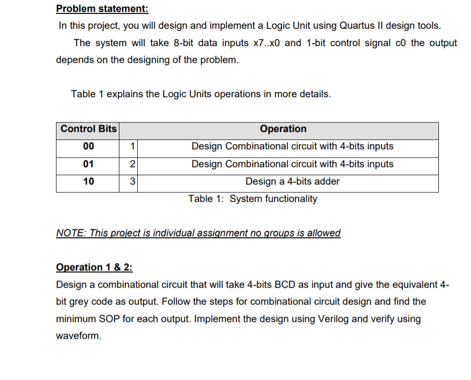
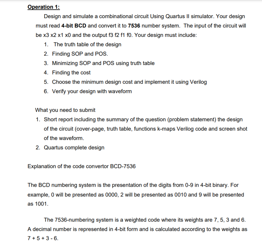
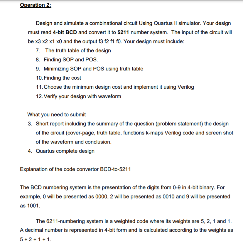
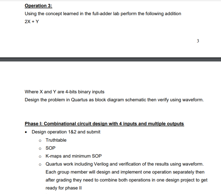
Problem statement: In this project, you will design and implement a Logic Unit using Quartus II design tools. The system will take 8-bit data inputs x7..x0 and 1-bit control signal co the output depends on the designing of the problem. Table 1 explains the Logic Units operations in more details. Control Bits 00 1 01 2 2 3 Operation Design Combinational circuit with 4-bits inputs Design Combinational circuit with 4-bits inputs Design a 4-bits adder Table 1: System functionality 10 NOTE: This project is individual assignment no groups is allowed Operation 1 & 2: Design a combinational circuit that will take 4-bits BCD as input and give the equivalent 4- bit grey code as output. Follow the steps for combinational circuit design and find the minimum SOP for each output. Implement the design using Verilog and verify using waveform. Operation 1: Design and simulate a combinational circuit Using Quartus Il simulator. Your design must read 4-bit BCD and convert it to 7536 number system. The input of the circuit will be x3 x2 x1 x0 and the output f3 f2 f1 fo. Your design must include: 1. The truth table of the design 2. Finding SOP and POS. 3. Minimizing SOP and POS using truth table 4. Finding the cost 5. Choose the minimum design cost and implement it using Verilog 6. Verify your design with waveform What you need to submit 1. Short report including the summary of the question (problem statement) the design of the circuit (cover-page, truth table, functions k-maps Verilog code and screen shot of the waveform. 2. Quartus complete design Explanation of the code convertor BCD-7536 The BCD numbering system is the presentation of the digits from 0-9 in 4-bit binary. For example, 0 will be presented as 0000, 2 will be presented as 0010 and 9 will be presented as 1001. The 7536-numbering system is a weighted code where its weights are 7,5, 3 and 6. A decimal number is represented in 4-bit form and is calculated according to the weights as 7 + 5 + 3 - 6. Operation 2: Design and simulate a combinational circuit Using Quartus Il simulator. Your design must read 4-bit BCD and convert it to 5211 number system. The input of the circuit will be x3 x2 x1 x0 and the output f3 f2 f1 fo. Your design must include: 7. The truth table of the design 8. Finding SOP and POS. 9. Minimizing SOP and POS using truth table 10. Finding the cost 11. Choose the minimum design cost and implement it using Verilog 12. Verify your design with waveform What you need to submit 3. Short report including the summary of the question (problem statement) the design of the circuit (cover-page, truth table, functions k-maps Verilog code and screen shot of the waveform and conclusion. 4. Quartus complete design Explanation of the code convertor BCD-to-5211 The BCD numbering system is the presentation of the digits from 0-9 in 4-bit binary. For example, 0 will be presented as 0000, 2 will be presented as 0010 and 9 will be presented as 1001. The 6211-numbering system is a weighted code where its weights are 5, 2, 1 and 1. A decimal number is represented in 4-bit form and is calculated according to the weights as 5 + 2 + 1 + 1. Operation 3: Using the concept learned in the full-adder lab perform the following addition 2X + Y 3 Where X and Y are 4-bits binary inputs Design the problem in Quartus as block diagram schematic then verify using waveform. Phase I: Combinational circuit design with 4 inputs and multiple outputs Design operation 1&2 and submit o Truthtable O SOP o K-maps and minimum SOP o Quartus work including Verilog and verification of the results using waveform. Each group member will design and implement one operation separately then after grading they need to combine both operations in one design project to get ready for phase II ready for phase II Phase II: full adders Design Operation 2 and submit o Your design work in word o Quartus work including all files with verification of results using waveforms Phase III: Integration of operations 1, 2 & 3 using mux In this part you will integrate operation 1, 2 and 3 using multiplexer. Then verify the final design using waveform. Problem statement: In this project, you will design and implement a Logic Unit using Quartus II design tools. The system will take 8-bit data inputs x7..x0 and 1-bit control signal co the output depends on the designing of the problem. Table 1 explains the Logic Units operations in more details. Control Bits 00 1 01 2 2 3 Operation Design Combinational circuit with 4-bits inputs Design Combinational circuit with 4-bits inputs Design a 4-bits adder Table 1: System functionality 10 NOTE: This project is individual assignment no groups is allowed Operation 1 & 2: Design a combinational circuit that will take 4-bits BCD as input and give the equivalent 4- bit grey code as output. Follow the steps for combinational circuit design and find the minimum SOP for each output. Implement the design using Verilog and verify using waveform. Operation 1: Design and simulate a combinational circuit Using Quartus Il simulator. Your design must read 4-bit BCD and convert it to 7536 number system. The input of the circuit will be x3 x2 x1 x0 and the output f3 f2 f1 fo. Your design must include: 1. The truth table of the design 2. Finding SOP and POS. 3. Minimizing SOP and POS using truth table 4. Finding the cost 5. Choose the minimum design cost and implement it using Verilog 6. Verify your design with waveform What you need to submit 1. Short report including the summary of the question (problem statement) the design of the circuit (cover-page, truth table, functions k-maps Verilog code and screen shot of the waveform. 2. Quartus complete design Explanation of the code convertor BCD-7536 The BCD numbering system is the presentation of the digits from 0-9 in 4-bit binary. For example, 0 will be presented as 0000, 2 will be presented as 0010 and 9 will be presented as 1001. The 7536-numbering system is a weighted code where its weights are 7,5, 3 and 6. A decimal number is represented in 4-bit form and is calculated according to the weights as 7 + 5 + 3 - 6. Operation 2: Design and simulate a combinational circuit Using Quartus Il simulator. Your design must read 4-bit BCD and convert it to 5211 number system. The input of the circuit will be x3 x2 x1 x0 and the output f3 f2 f1 fo. Your design must include: 7. The truth table of the design 8. Finding SOP and POS. 9. Minimizing SOP and POS using truth table 10. Finding the cost 11. Choose the minimum design cost and implement it using Verilog 12. Verify your design with waveform What you need to submit 3. Short report including the summary of the question (problem statement) the design of the circuit (cover-page, truth table, functions k-maps Verilog code and screen shot of the waveform and conclusion. 4. Quartus complete design Explanation of the code convertor BCD-to-5211 The BCD numbering system is the presentation of the digits from 0-9 in 4-bit binary. For example, 0 will be presented as 0000, 2 will be presented as 0010 and 9 will be presented as 1001. The 6211-numbering system is a weighted code where its weights are 5, 2, 1 and 1. A decimal number is represented in 4-bit form and is calculated according to the weights as 5 + 2 + 1 + 1. Operation 3: Using the concept learned in the full-adder lab perform the following addition 2X + Y 3 Where X and Y are 4-bits binary inputs Design the problem in Quartus as block diagram schematic then verify using waveform. Phase I: Combinational circuit design with 4 inputs and multiple outputs Design operation 1&2 and submit o Truthtable O SOP o K-maps and minimum SOP o Quartus work including Verilog and verification of the results using waveform. Each group member will design and implement one operation separately then after grading they need to combine both operations in one design project to get ready for phase II ready for phase II Phase II: full adders Design Operation 2 and submit o Your design work in word o Quartus work including all files with verification of results using waveforms Phase III: Integration of operations 1, 2 & 3 using mux In this part you will integrate operation 1, 2 and 3 using multiplexer. Then verify the final design using waveform
Step by Step Solution
There are 3 Steps involved in it

Get step-by-step solutions from verified subject matter experts