

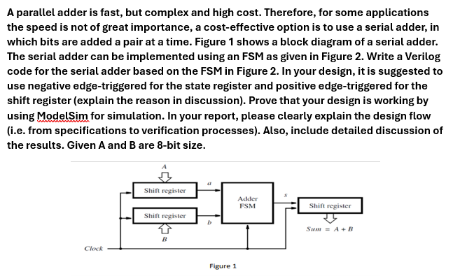
Question: A parallel adder is fast, but complex and high cost. Therefore, for some applications the speed is not of great importance, a cost - effective
A parallel adder is fast, but complex and high cost. Therefore, for some applications the speed is not of great importance, a costeffective option is to use a serial adder, in which bits are added a pair at a time. Figure shows a block diagram of a serial adder. The serial adder can be implemented using an FSM as given in Figure Write a Verilog code for the serial adder based on the FSM in Figure In your design, it is suggested to use negative edgetriggered for the state register and positive edgetriggered for the shift register explain the reason in discussion Prove that your design is working by using ModelSim for simulation. In your report, please clearly explain the design flow ie from specifications to verification processes Also, include detailed discussion of the results. Given A and B are bit size. Write Verilog HDL code for this Figure Write Verilog code HDL testbench and attach picture Simulation waveform bit as question required. Need write codes. Make sure the code is correct with Quart's prime and upload picture of the result and Simulation waveform bit Pls if u do not know the answer leave it to Somone can answer do not answer it wrong. becesue, I pay money to post this question.
Subject is Programmable Electronics
Step by Step Solution
There are 3 Steps involved in it
1 Expert Approved Answer
Step: 1 Unlock

Question Has Been Solved by an Expert!
Get step-by-step solutions from verified subject matter experts
Step: 2 Unlock
Step: 3 Unlock