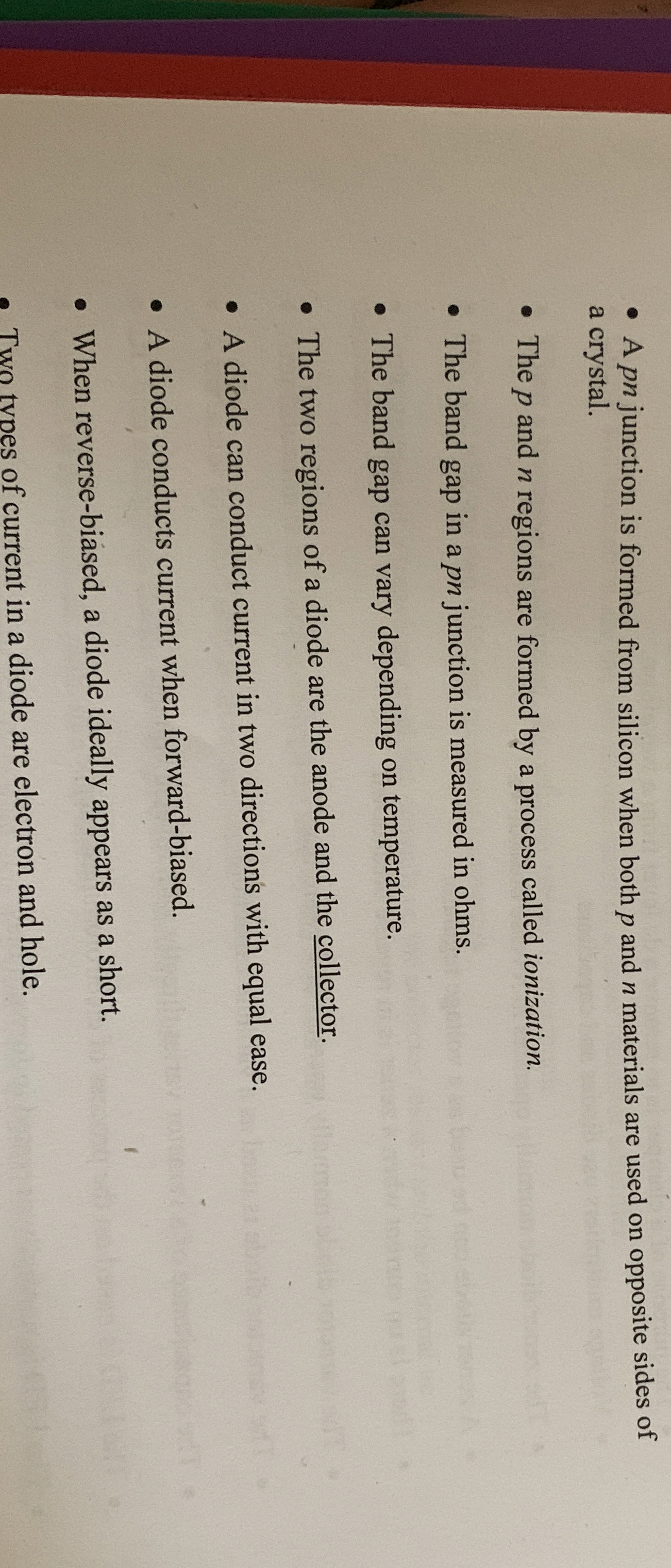
Question: A pn junction is formed from silicon when both p and n materials are used on opposite sides of a crystal. The p and n
A pn junction is formed from silicon when both and materials are used on opposite sides of a crystal.
The and regions are formed by a process called ionization.
The band gap in a pn junction is measured in ohms.
The band gap can vary depending on temperature.
The two regions of a diode are the anode and the collector.
A diode can conduct current in two directions with equal ease.
A diode conducts current when forwardbiased.
When reversebiased, a diode ideally appears as a short.
Two tvnes of current in a diode are electron and hole.

Step by Step Solution
There are 3 Steps involved in it
1 Expert Approved Answer
Step: 1 Unlock


Question Has Been Solved by an Expert!
Get step-by-step solutions from verified subject matter experts
Step: 2 Unlock
Step: 3 Unlock


