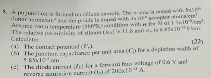
Question: 3. A pn junction is formed on silicon sample. The n-side is doped with 51016 donor atoms /cm3 and the p-side is doped with 31018

3. A pn junction is formed on silicon sample. The n-side is doped with 51016 donor atoms /cm3 and the p-side is doped with 31018 acceptor atoms /cm3. Assume room temperature (300K) condition with ni for Si of 1.51010/cm3. The relative permittivity of silicon (si) is 11.8 and is 8.851014F/cm. Calculate: (a) The contact potential (Vo). (b) The junction capacitance per unit area (Cj) for a depletion width of 5.85105cm. (c) The diode current (ID) for a forward bias voltage of 0.6V and reverse saturation current (IS) of 2001015A. 3. A pn junction is formed on silicon sample. The n-side is doped with 51016 donor atoms /cm3 and the p-side is doped with 31018 acceptor atoms /cm3. Assume room temperature (300K) condition with ni for Si of 1.51010/cm3. The relative permittivity of silicon (si) is 11.8 and is 8.851014F/cm. Calculate: (a) The contact potential (Vo). (b) The junction capacitance per unit area (Cj) for a depletion width of 5.85105cm. (c) The diode current (ID) for a forward bias voltage of 0.6V and reverse saturation current (IS) of 2001015A
Step by Step Solution
There are 3 Steps involved in it

Get step-by-step solutions from verified subject matter experts


