

Question: (a) (b) (c) (c) What is the typical FPGA hardware design flow when VHDL is used as the design entry? In an FPGA, memories
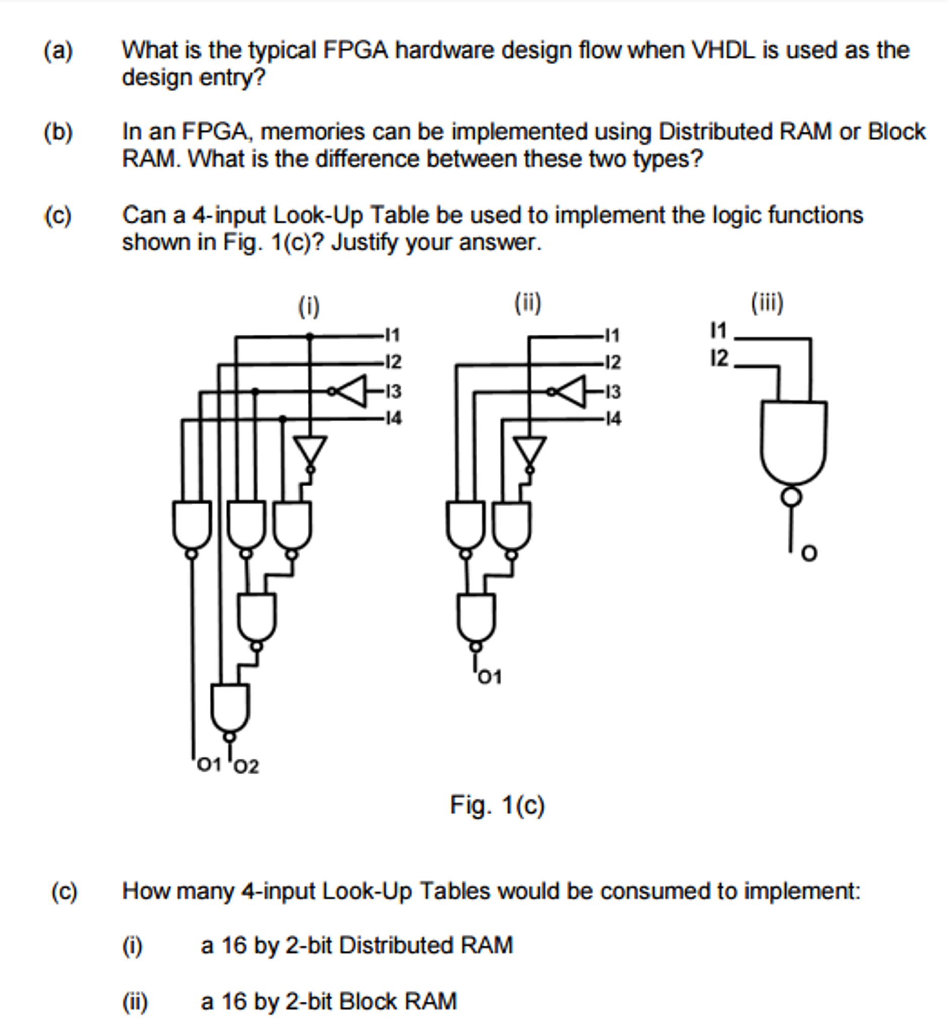
(a) (b) (c) (c) What is the typical FPGA hardware design flow when VHDL is used as the design entry? In an FPGA, memories can be implemented using Distributed RAM or Block RAM. What is the difference between these two types? Can a 4-input Look-Up Table be used to implement the logic functions shown in Fig. 1(c)? Justify your answer. (1) (ii) 01'02 1234 01 Fig. 1(c) -11 234 11 12 How many 4-input Look-Up Tables would be consumed to implement: (1) a 16 by 2-bit Distributed RAM a 16 by 2-bit Block RAM
Step by Step Solution
3.40 Rating (150 Votes )
There are 3 Steps involved in it
To answer your questions lets break them down step by step a Typical FPGA Hardware Design Flow Using VHDL 1 Design Entry Write the initial design usin... View full answer

Get step-by-step solutions from verified subject matter experts