

Question: 2.7 Based upon the discussion in Section 2.4, what is the smallest feature size F that can be reproduced with a 193-nm optical source?
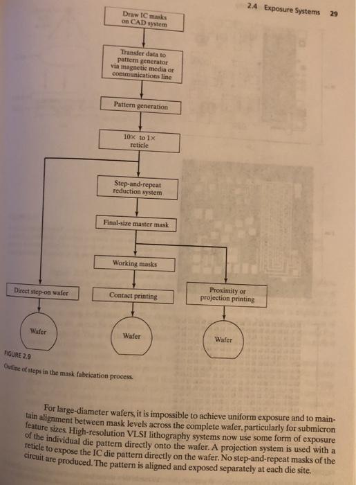
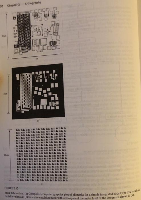
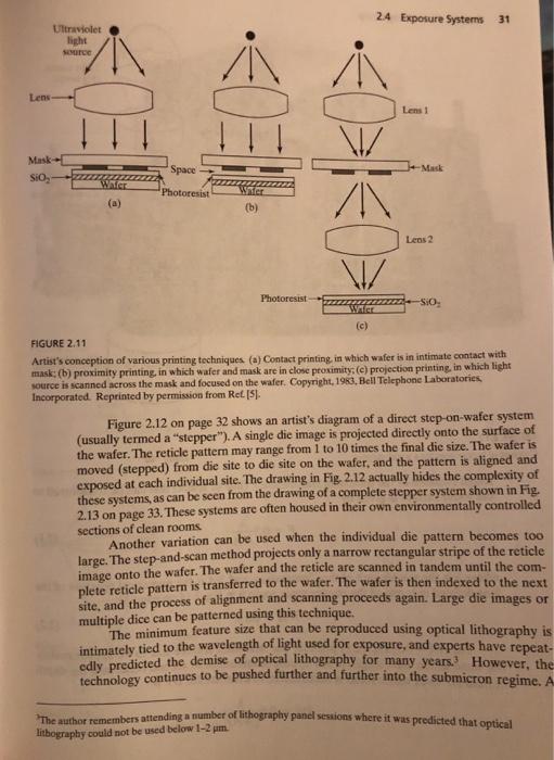
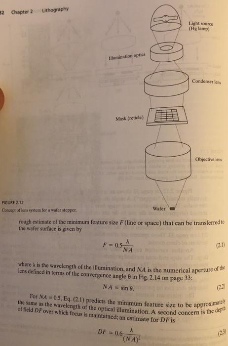
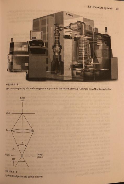
2.7 Based upon the discussion in Section 2.4, what is the smallest feature size F that can be reproduced with a 193-nm optical source? 2.8 An extreme ultra violet (EUV) lithography source uses a 13-nm exposure wavelength. Based upon the discussion in Section 2.4, what is the smallest feature size F that can be reproduced with this courgo? 2.4 EXPOSURE SYSTEMS Because contact printing can damage the surfaces of both the mask and the wafer, manu- facturing lines utilize proximity and projection printing systems, as illustrated in Fig. 2.11. However, contact printing is still used in research and prototyping situations, because it can economically achieve high-resolution pattern transfer. In proximity printing, the mask is brought in very close proximity to the wafer, but does not come in contact with the wafer during exposure, thus preventing damage to the mask. Projection printing uses a dual-lens system to project a portion of the mask image onto the wafer surface. The wafer and masks may be scanned, or the system may operate in a step-and-repeat mode. The actual mask and lenses are mounted many centimeters from the wafer surface. Direct step-on wafer Wafer Draw IC masks on CAD system Transfer data to pattern generator via magnetic media or communications line Pattern generation 10x to 1x reticle Step-and-repeat reduction system Final-size master mask Working masks Contact printing Wafer FIGURE 2.9 Outline of steps in the mask fabrication process. 2.4 Exposure Systems 29 Wafer 10 Proximity or projection printing For large-diameter wafers, it is impossible to achieve uniform exposure and to main- tain alignment between mask levels across the complete wafer, particularly for submicron feature sizes. High-resolution VLSI lithography systems now use some form of exposure of the individual die pattern directly onto the wafer. A projection system is used with a reticle to expose the IC die pattern directly on the wafer. No step-and-repeat masks of the circuit are produced. The pattern is aligned and exposed separately at each die site. 30 Chapter 2 2 mm 10 cm Lithography 7000 Sai La la la la la l LLLLLL El la la la l ELLEL EELLE! BEEEEE LLEEL CELLE GEELE BELLE LLLLLE Ti 1 1 1 1 La la la la la T BELLLE Le Le La La La L La La La La La Le Le Le Le La LaLL AUEE 7910 (c) Lakel 1 1 1 1 L FL GRL h ELLE Is It La LLL la l la T l LLLLLL FIGURE 2.10 Mask fabrication. (a) Composite computer graphics plot of all masks for a simple integrated circuit; (b) 10X reticle of metal-level mask; (c) final-size emulsion mask with 400 copies of the metal level of the integrated circuit in (a). Ultraviolet light source Lens- Mask SIO M Water (a) Space Photoresist A Water (b) Photoresist 2.4 Exposure Systems 31 \/ AN \/ Wifer (c) Lens 1 -Mask Lens 2 -SiO FIGURE 2.11 Artist's conception of various printing techniques. (a) Contact printing, in which wafer is in intimate contact with mask: (b) proximity printing, in which wafer and mask are in close proximity; (c) projection printing, in which light source is scanned across the mask and focused on the wafer. Copyright, 1983, Bell Telephone Laboratories Incorporated. Reprinted by permission from Ref. [5]. Figure 2.12 on page 32 shows an artist's diagram of a direct step-on-wafer system (usually termed a "stepper"). A single die image is projected directly onto the surface of the wafer. The reticle pattern may range from 1 to 10 times the final die size. The wafer is moved (stepped) from die site to die site on the wafer, and the pattern is aligned and exposed at each individual site. The drawing in Fig. 2.12 actually hides the complexity of these systems, as can be seen from the drawing of a complete stepper system shown in Fig. 2.13 on page 33. These systems are often housed in their own environmentally controlled sections of clean rooms. Another variation can be used when the individual die pattern becomes too large. The step-and-scan method projects only a narrow rectangular stripe of the reticle image onto the wafer. The wafer and the reticle are scanned in tandem until the com- plete reticle pattern is transferred to the wafer. The wafer is then indexed to the next site, and the process of alignment and scanning proceeds again. Large die images or multiple dice can be patterned using this technique. The minimum feature size that can be reproduced using optical lithography is intimately tied to the wavelength of light used for exposure, and experts have repeat- edly predicted the demise of optical lithography for many years. However, the technology continues to be pushed further and further into the submicron regime. A The author remembers attending a number of lithography panel sessions where it was predicted that optical lithography could not be used below 1-2 um. 32 Chapter 2 Lithography FIGURE 2.12 Concept of lens system for a water stepper. Illumination optics Mask (reticle) F = 0.5- 000 DF= 0.6 Wafer rough estimate of the minimum feature size F (line or space) that can be transferred to the wafer surface is given by A (NA) Light source (Hg lamp) Condenser lens Objective lens where A is the wavelength of the illumination, and NA is the numerical aperture of the lens defined in terms of the convergence angle 8 in Fig. 2.14 on page 33: NA = sin 8. (2.1) For NA=0.5, Eq. (2.1) predicts the minimum feature size to be approximately the same as the wavelength of the optical illumination. A second concern is the depth of field DF over which focus is maintained; an estimate for DF is (22) (2.3) Mask Lens FIGURE 2.13 The true complexity of a water stepper is apparent in this system drawing (Courtesy of ASM Lithography, Inc.) Water DF Lens axis Image plane ASMIL FIGURE 2.14 Optical focal plane and depth of focus 2.4 Exposure Systems 33 PAG-2800 NE 4 Chapter 2 Lithography Based upon Eqs. (2.1) and (2.3) with NA=0.5, one-tenth-micron technology (F= 0.10 m) would require a 100-nm illumination source and have only a 240 nm (0.24 m) depth of field. Thus, wafer planarity at each exposure step represents a critical issue, since focus will be maintained over a distance of only 0.12 m from the primary focal plane.
Step by Step Solution
3.54 Rating (171 Votes )
There are 3 Steps involved in it

Get step-by-step solutions from verified subject matter experts