

Question: Address lines Row address Column address RAS - - CAS R/W - - - ----- Data lines Data out valid - Figure 5.20 Simplified DRAM
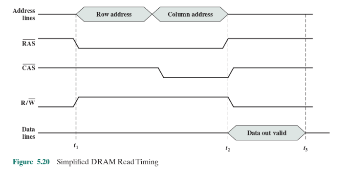
Address lines Row address Column address RAS - - CAS R/W - - - ----- Data lines Data out valid - Figure 5.20 Simplified DRAM Read Timing 5.3 Figure 5.20 shows a simplified timing diagram for a DRAM read operation over a bus. The access time is considered to last from ti to t2. Then there is a recharge time, lasting from t2 to tz, during which the DRAM chips will have to recharge before the processor can access them again. 225/2020 1:37:58 PM-429813K-92.96.43.175 a. Assume that the access time is 151 ns and the recharge time is 49 ns. What is the memory cycle time? What is the maximum data rate this DRAM can sustain, assuming a 2-bit output, and a 4-bit output? b. Constructing a 64-bit wide memory system using these chips yields what data transfer rate
Step by Step Solution
There are 3 Steps involved in it

Get step-by-step solutions from verified subject matter experts