

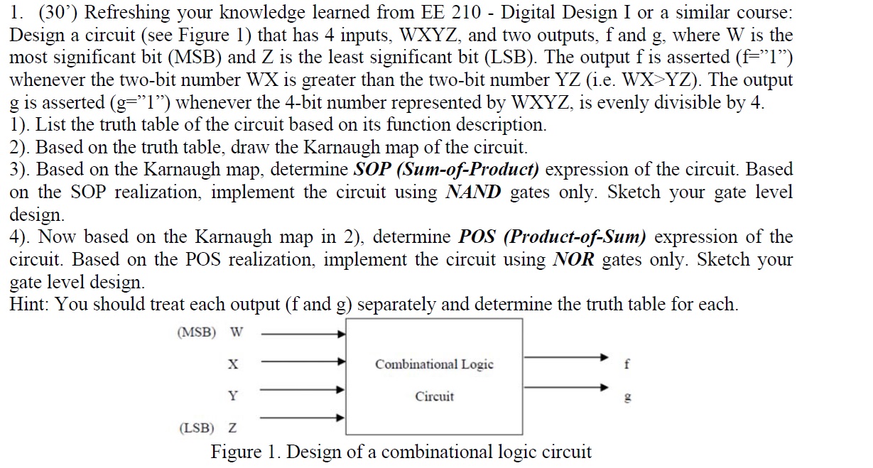
Question: ask to an expert the pdf 1 . ( ( 3 0 ) ' ) Refreshing your knowledge learned from EE 2 1
ask to an expert the pdf Refreshing your knowledge learned from EE Digital Design I or a similar course: Design a circuit see Figure that has inputs, WXYZ and two outputs, f and g where W is the most significant bit MSB and Z is the least significant bit LSB The output f is asserted mathrmf whenever the twobit number WX is greater than the twobit number YZ ie WXYZ The output g is asserted mathrmg whenever the bit number represented by WXYZ is evenly divisible by
List the truth table of the circuit based on its function description.
Based on the truth table, draw the Karnaugh map of the circuit.
Based on the Karnaugh map, determine SOP SumofProduct expression of the circuit. Based on the SOP realization, implement the circuit using boldsymbolN A N D gates only. Sketch your gate level design.
Now based on the Karnaugh map in determine POS ProductofSum expression of the circuit. Based on the POS realization, implement the circuit using NOR gates only. Sketch your gate level design.
Hint: You should treat each outnut f and sigma senarately and determine the truth tahle for each.
Figure Design of a combinational logic circuit
Step by Step Solution
There are 3 Steps involved in it
1 Expert Approved Answer
Step: 1 Unlock

Question Has Been Solved by an Expert!
Get step-by-step solutions from verified subject matter experts
Step: 2 Unlock
Step: 3 Unlock