

Question: The NMOS transistor in the common gate amplifier circuit shown has the following parameters: = 0 kn = 500 A/V VTH = 1 V
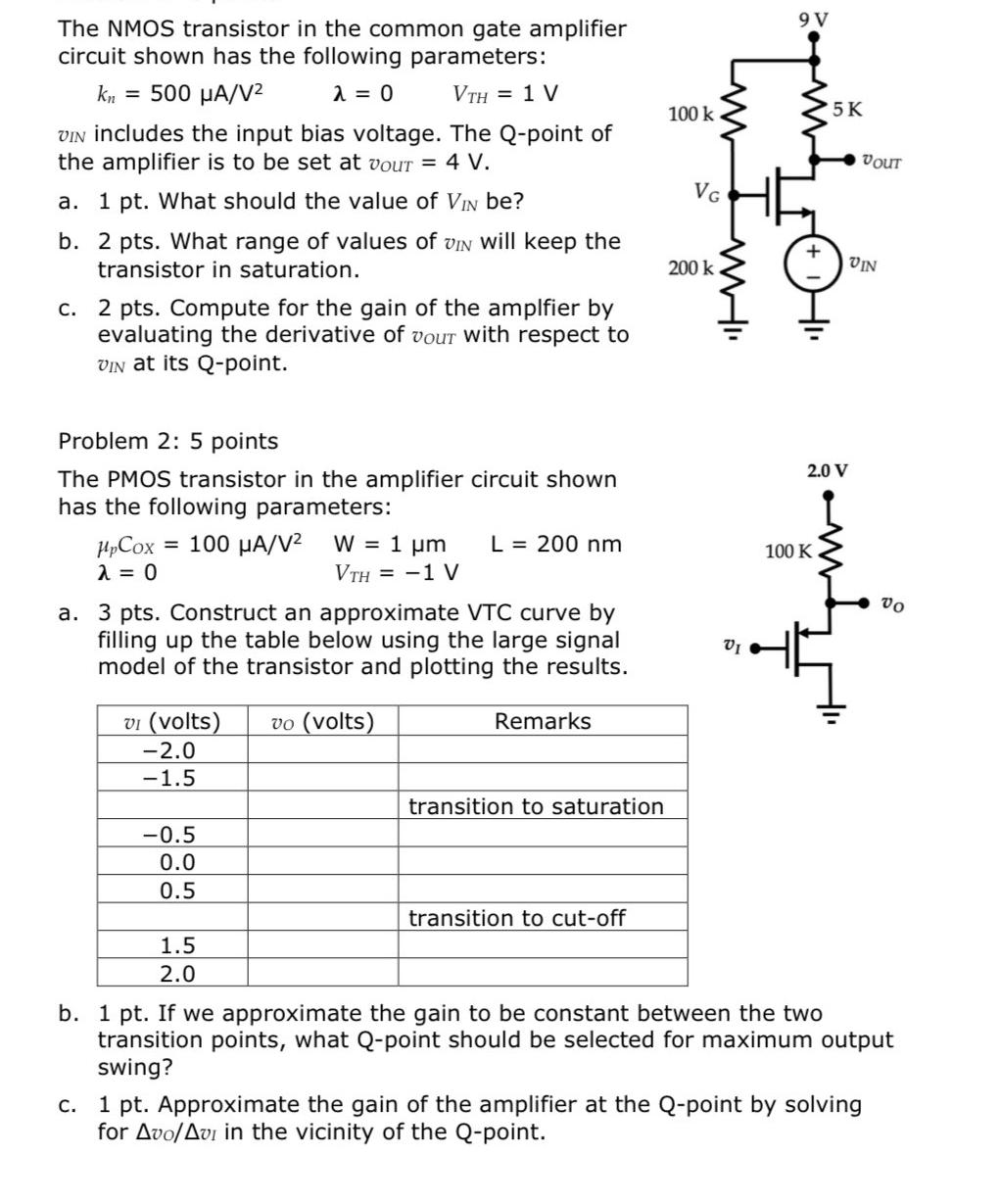
The NMOS transistor in the common gate amplifier circuit shown has the following parameters: = 0 kn = 500 A/V VTH = 1 V VIN includes the input bias voltage. The Q-point of the amplifier is to be set at your = 4 V. a. 1 pt. What should the value of VIN be? b. 2 pts. What range of values of VIN will keep the transistor in saturation. c. 2 pts. Compute for the gain of the amplfier by evaluating the derivative of your with respect to VIN at its Q-point. Problem 2: 5 points The PMOS transistor in the amplifier circuit shown has the following parameters: pCox = 100 A/V = 0 Vi (volts) -2.0 -1.5 a. 3 pts. Construct an approximate VTC curve by filling up the table below using the large signal model of the transistor and plotting the results. vo (volts) -0.5 0.0 0.5 W = 1 m VTH = -1 V 1.5 2.0 L 200 nm Remarks transition to saturation transition to cut-off 100 k VG 200 k Iw". VI 9V 5 K 2.0 V www. 100 K -1 VOUT VIN c. 1 pt. Approximate the gain of the amplifier at the Q-point by solving for Avo/Avi in the vicinity of the Q-point. Vo b. 1 pt. If we approximate the gain to be constant between the two transition points, what Q-point should be selected for maximum output swing?
Step by Step Solution
3.48 Rating (161 Votes )
There are 3 Steps involved in it
Part a To find the value ofVmwe need to use the DC transfer curve of the NMOS transistorThis curve shows the relationship between the drainsource voltageVDSand the drain currentIDfor a given gatesourc... View full answer

Get step-by-step solutions from verified subject matter experts