

Question: Combinational Logic Using Verilog QUESTIONS AND PROBLEMS 8.1 Write the Verilog module header for the block diagram shown in Figure P8.1. FIGURE P8.1 Write
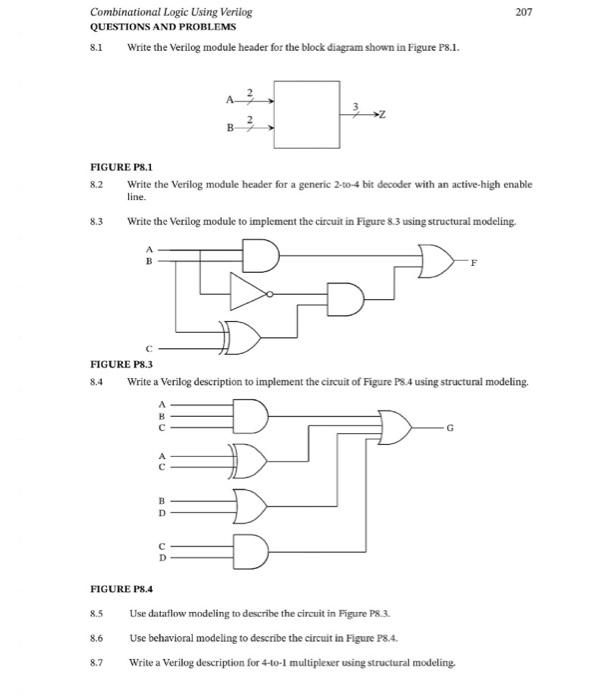
Combinational Logic Using Verilog QUESTIONS AND PROBLEMS 8.1 Write the Verilog module header for the block diagram shown in Figure P8.1. FIGURE P8.1 Write the Verilog module header for a generic 2-to-4 bit decoder with an active-high enable line. Write the Verilog module to implement the circuit in Figure 8.3 using structural modeling. 8.2 8.3 C FIGURE P8.3 8.4 Write a Verilog description to implement the circuit of Figure P8.4 using structural modeling. FIGURE P8.4 8.5 A B 8.6 8.7 A B 40 BD D 207 G Use dataflow modeling to describe the circuit in Figure P8.3. Use behavioral modeling to describe the circuit in Figure P8.4. Write a Verilog description for 4-to-1 multiplexer using structural modeling.
Step by Step Solution
3.60 Rating (154 Votes )
There are 3 Steps involved in it

Get step-by-step solutions from verified subject matter experts