

Question: Consider a silicon pn junction with the doping profile shown in Figure P7.29. T = 300 K (a) Calculated the applied reverse-biased voltage required so
Consider a silicon pn junction with the doping profile shown in Figure P7.29.
T = 300 K
(a) Calculated the applied reverse-biased voltage required so that the space charge region extends entirely through the p region.
(b) Determine the space charge width into the n+ region with the reverse-biased voltage calculated in part (a).
(c) Calculate the peak electric field for this applied voltage 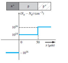
1016 1014 P +(Ng Ng) (cm^3) 0 2016 50 x ()
Step by Step Solution
3.33 Rating (156 Votes )
There are 3 Steps involved in it
To solve this problem well follow these steps a Calculate the applied reversebiased voltage VR requi... View full answer

Get step-by-step solutions from verified subject matter experts