

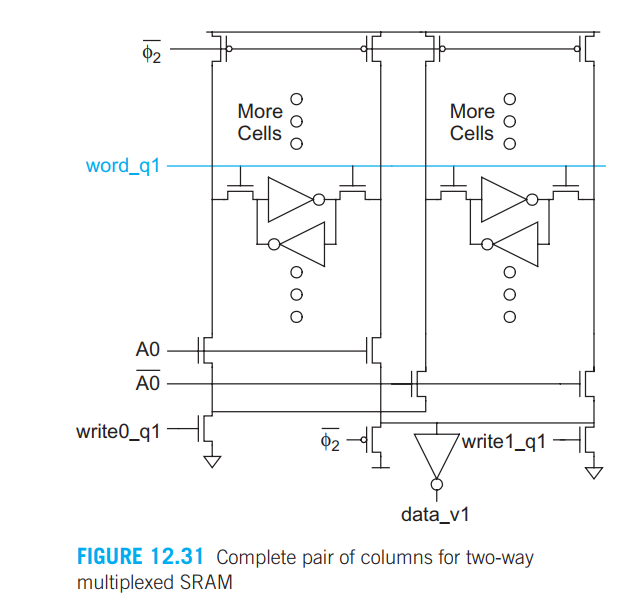
Question: Consider the circuit in Fig. 1 2 . 3 1 from CMOS VLSI Design book ( 4 th Edition ) by Neil H . E
Consider the circuit in Fig. from CMOS VLSI Design
book th Edition by Neil H E Weste and David Money Harris. Propose a set of transistor sizes for all the MOSFETs in the precharge, read, write circuitry and the sram cell itself. Make sure you have considered writeabilty and read stability Estimate the delay to precharge a bit line assuming there are cells in the column. Assume diffusion capacitance of a MOSFET is equal to its gate capacitance. Assume np Estimate the time it takes to discharge a bit line to Vdd Express delays in multiples of a MOSFETs RC delay.
FIGURE Complete pair of columns for twoway
multiplexed SRAM
Step by Step Solution
There are 3 Steps involved in it
1 Expert Approved Answer
Step: 1 Unlock

Question Has Been Solved by an Expert!
Get step-by-step solutions from verified subject matter experts
Step: 2 Unlock
Step: 3 Unlock