

Question: Consider the CMOS circuit below, with three inputs V1, V2, and V3. and one output Vout. The source terminal of the PMOS at the upper
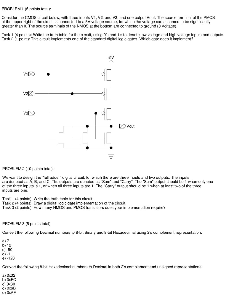
Consider the CMOS circuit below, with three inputs V1, V2, and V3. and one output Vout. The source terminal of the PMOS at the upper right of the circuit is connected to a 5V voltage source, for which the voltage can assumed to be significantly greater than 0. The source terminals of the NMOS at the bottom are connected to ground (0 Voltage). Task 1 : Write the truth table for the circuit, using 0's and 1's to denote low voltage and high voltage inputs and outputs. Task 2: This circuit implements one of the standard digital logic gates. Which gate does it implement? We want to design the 'lull adder" digital circuit, for which there are three inputs and two outputs. The inputs are denoted as A, B, and C. The outputs are denoted as "Sum" and "Carry". The "Sum" output should be 1 when only one of the three inputs is 1, or when all three inputs are 1. The "Carry" output should be 1 when at least two of the three inputs are one. Task 1: Write the truth table for this circuit. Task 2: Draw a digital logic gate implementation of the circuit. Task 3: How many NMOS and PMOS transistors does your implementation require? Convert the following Decimal numbers to 8-bit Binary and 8-bit Hexadecimal using 2's complement representation: a) 7 b) 12 c) -50 d) -1 e) -128 Convert the following 8-bit Hexadecimal numbers to Decimal in both 2's complement and unsigned representations: a) 0 times 32 b) 0 times FC c) 0 times 80 d) 0 times 6B e) 0times AF
Step by Step Solution
There are 3 Steps involved in it

Get step-by-step solutions from verified subject matter experts