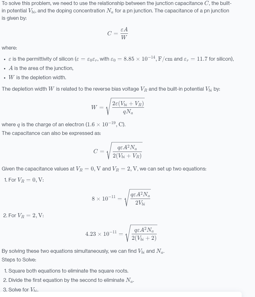
Question: continuie this: To solve this problem, we need to use the relationship between the junction capacitance ', the built- in potential V3;, and the doping

continuie this:

continuie this: To solve this problem, we need to
To solve this problem, we need to use the relationship between the junction capacitance ', the built- in potential V3;, and the doping concentration N, for a pn junction. The capacitance of a pn junction is given by: 4 W where: is the permittivity of silicon (= = e,., with g 8.85 x 10714, F/cm and g, = 11.7 for silicon), A is the area of the junction, W is the depletion width. The depletion width W is related to the reverse bias voltage Vg and the built-in potential V3,; by: 2(Vhi + Vi) W = gN, where is the charge of an electron (1.6 x 1071, C). The capacitance can also be expressed as: g AN, e B G U 2(Vei + VR) Given the capacitance values at V = 0, V and Vi = 2, V, we can set up two equations: 1L.ForVp =0,V: B geA2N, 8 x 10~ = 4/ "a - 2V 2.ForVp =2,V: cA2N, 493 x 1070 =,/ L2 Te 2(Vii + 2) By solving these two equations simultaneously, we can find V3; and N,. Steps to Solve: 1. Square both equations to eliminate the square roots. 2. Divide the first equation by the second to eliminate V. 3. Solve for V

Step by Step Solution

There are 3 Steps involved in it

1 Expert Approved Answer
Step: 1 Unlock blur-text-image
Question Has Been Solved by an Expert!

Get step-by-step solutions from verified subject matter experts

Step: 2 Unlock
Step: 3 Unlock

Students Have Also Explored These Related Business Writing Questions!