

Question: CPU TIMING DIAGRAM ( part 1 ) Note that this block diagram is only for reference, it is not needed to complete the exercise The
CPU TIMING DIAGRAM part
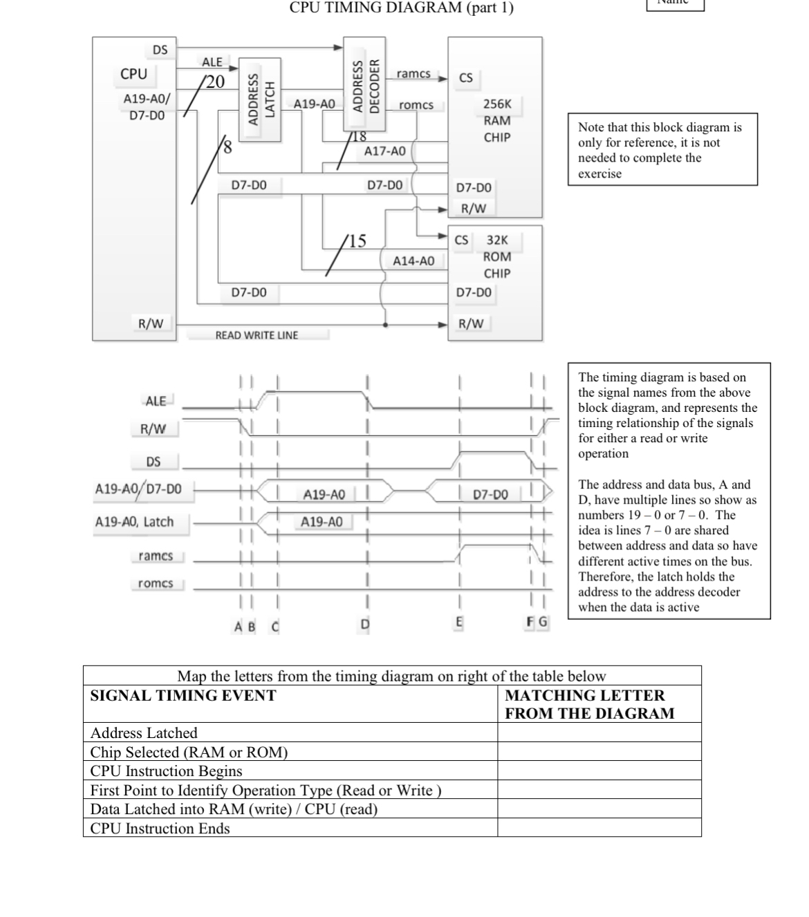
Note that this block diagram is only for reference, it is not needed to complete the exercise
The timing diagram is based on the signal names from the above block diagram, and represents the timing relationship of the signals for either a read or write operation
The address and data bus, A and have multiple lines so show as numbers or The idea is lines are shared between address and data so have different active times on the bus. Therefore, the latch holds the address to the address decoder when the data is active
tableMap the letters from the timing diagram on right of the table belowSIGNAL TIMING EVENT,tableMATCHING LETTERFROM THE DIAGRAMAddress Latched,Chip Selected RAM or ROMCPU Instruction Begins,First Point to Identify Operation Type Read or WriteData Latched into RAM write CPU readCPU Instruction Ends,
Step by Step Solution
There are 3 Steps involved in it
1 Expert Approved Answer
Step: 1 Unlock

Question Has Been Solved by an Expert!
Get step-by-step solutions from verified subject matter experts
Step: 2 Unlock
Step: 3 Unlock