

Question: CSC 2 6 8 Computer Organization Practice Exercise 7 . 2 Design a 3 - bit parallel load shift register using four T flip -
CSC Computer Organization
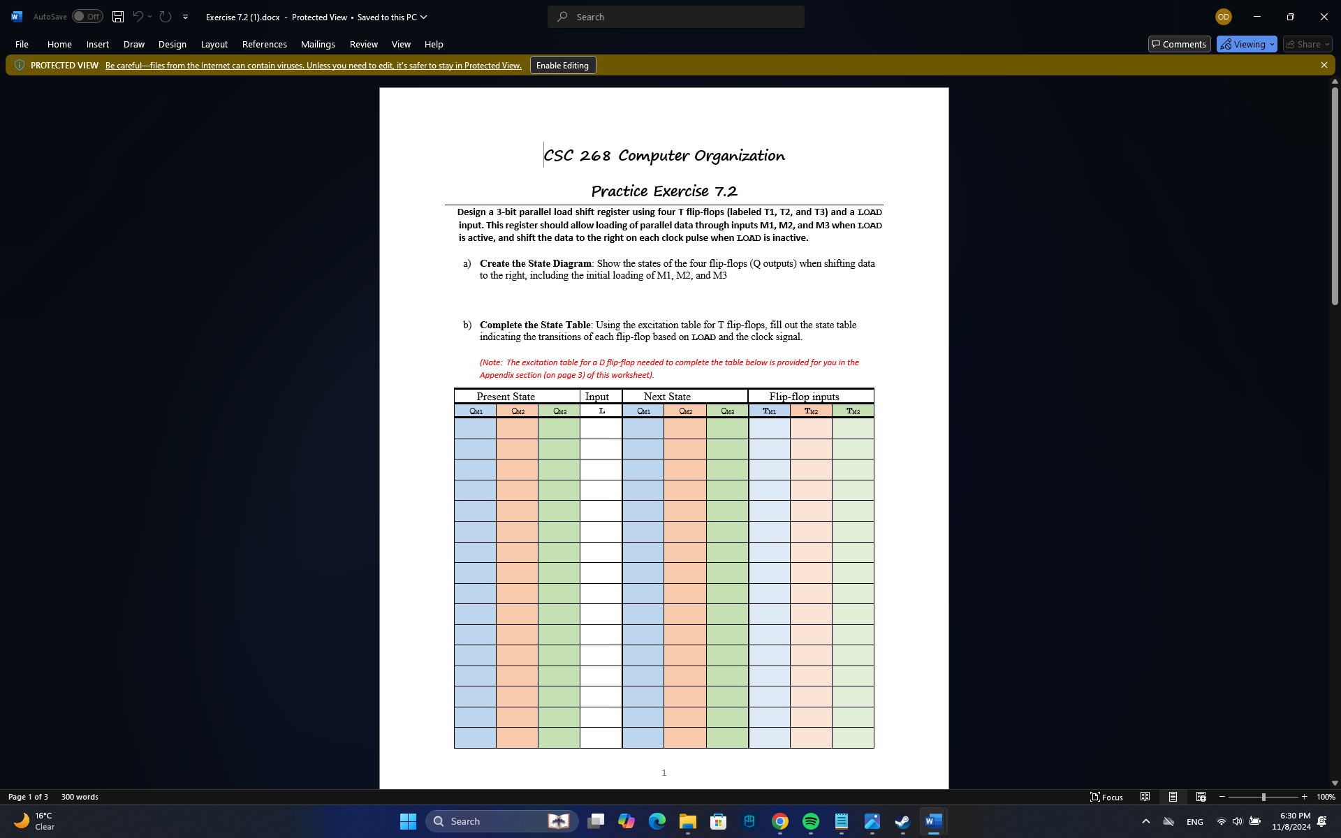
Practice Exercise
Design a bit parallel load shift register using four T flipflops labeled T T and T and a LOAD input. This register should allow loading of parallel data through inputs M M and M when LOAD is active, and shift the data to the right on each clock pulse when LOAD is inactive.
a Create the State Diagram: Show the states of the four flipflops Q outputs when shifting data to the right, including the initial loading of M M and M
b Complete the State Table: Using the excitation table for T flipflops, fill out the state table indicating the transitions of each flipflop based on LOAD and the clock signal.
Note: The excitation table for a D flipflop needed to complete the table below is provided for you in the Appendix section on page of this worksheet
begintabularcccccccccc
hline multicolumnlPresent State & Input & multicolumnlNext State & multicolumnlFlipflop inputs
hline mathrmQmathrmM & am & QM & L & mathrmOmathrmm & OM & & mathrmTmathrmM & mathrmTmathrmM & mathrmTmathrmM
hline & & & & & & & & &
hline & & & & & & & & &
hline & & & & & & & & &
hline & & & & & & & & &
hline & & & & & & & & &
hline & & & & & & & & &
hline & & & & & & & & &
hline & & & & & & & & &
hline & & & & & & & & &
hline & & & & & & & & &
hline & & & & & & & & &
hline & & & & & & & & &
hline & & & & & & & & &
hline & & & & & & & & &
hline & & & & & & & & &
hline & & & & & & & & &
hline
endtabular
c KMaps and Equations: Using the state transitions, complete the KMap for each flipflop input mathrmTmathrmMmathrm~TmathrmMmathrm~TmathrmM and derive the Boolean equations needed for the circuit design.
Note: the equation of a KMap with all s in the table is equal to
d Draw the Logic Circuit: Design the full circuit diagram with T flipflops and the logic gates required to achieve the parallel load and shift functionality.
Step by Step Solution
There are 3 Steps involved in it
1 Expert Approved Answer
Step: 1 Unlock

Question Has Been Solved by an Expert!
Get step-by-step solutions from verified subject matter experts
Step: 2 Unlock
Step: 3 Unlock