

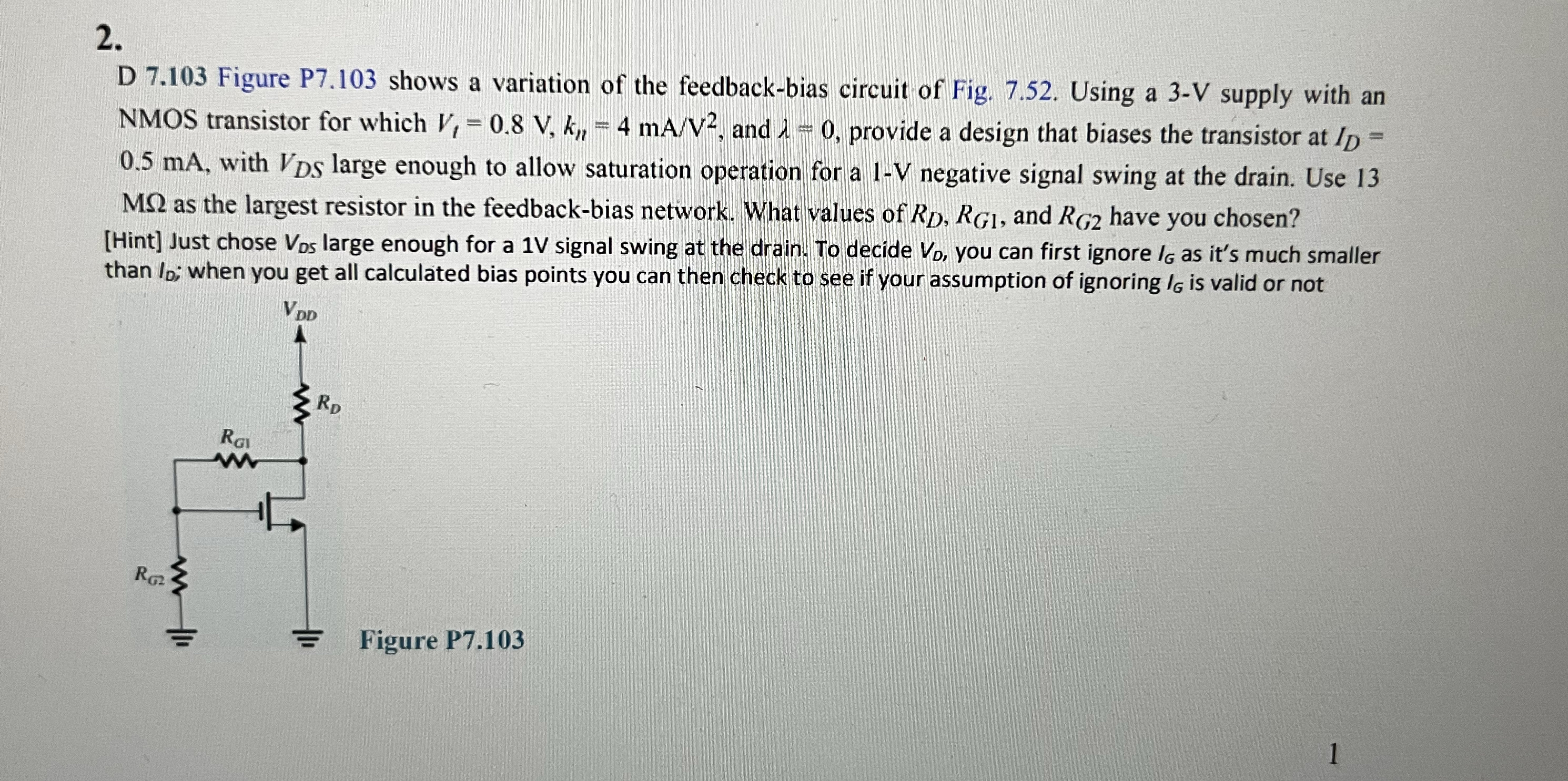
Question: D 7 . 1 0 3 Figure P 7 . 1 0 3 shows a variation of the feedback - bias circuit of Fig. 7
D Figure P shows a variation of the feedbackbias circuit of Fig. Using a V supply with an NMOS transistor for which and provide a design that biases the transistor at mA with large enough to allow saturation operation for a V negative signal swing at the drain. Use as the largest resistor in the feedbackbias network. What values of and have you chosen? Hint Just chose large enough for a V signal swing at the drain. To decide you can first ignore as it's much smaller than ; when you get all calculated bias points you can then check to see if your assumption of ignoring is valid or not
Step by Step Solution
There are 3 Steps involved in it
1 Expert Approved Answer
Step: 1 Unlock

Question Has Been Solved by an Expert!
Get step-by-step solutions from verified subject matter experts
Step: 2 Unlock
Step: 3 Unlock