

Question: d) Finally, the simulated Gain Margin (GM) and Phase Margin (PM) graphs for your designed circuit in Figure 2, as depicted in Figure 3. Validate
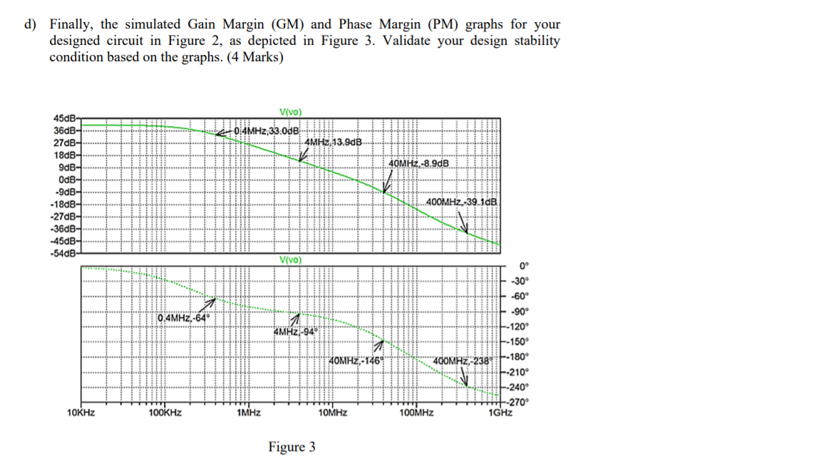
d) Finally, the simulated Gain Margin (GM) and Phase Margin (PM) graphs for your designed circuit in Figure 2, as depicted in Figure 3. Validate your design stability condition based on the graphs. (4 Marks) Vivo) 0.4MHz,33.0dB 4MHz, 13.9dB 40MHz -8.9dB 45dB 36dB- 27dB- 18dB- 9dB- OdB- -9dB - 18dB- -27dB- -36dB- -45dB- -54dB 400MHz-39.1dB Vivo) 0 0.4MHz,-64 4MHz -949 -30 -60 -90 -120 F-150 F-180 F-210 -240 40MHZ 1469 400MHZ-238 270 10KHz 100KHz 1 MHz 10MHz 100MHz 1GHz Figure 3
Step by Step Solution
There are 3 Steps involved in it
1 Expert Approved Answer
Step: 1 Unlock

Question Has Been Solved by an Expert!
Get step-by-step solutions from verified subject matter experts
Step: 2 Unlock
Step: 3 Unlock