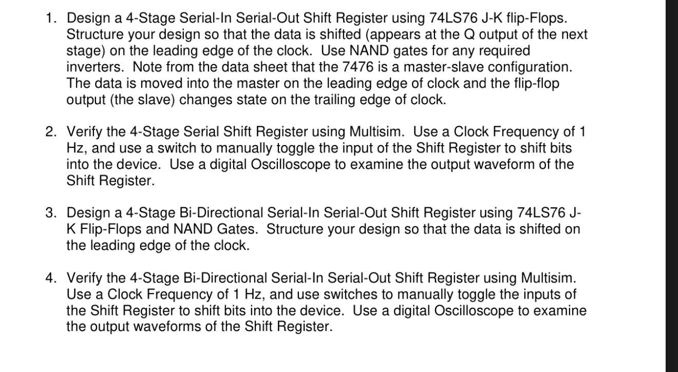
Question: Design a 4 - Stage Serial - In Serial - Out Shift Register using 7 4 LS 7 6 J - K flip - Flops.
Design a Stage SerialIn SerialOut Shift Register using LS JK flipFlops. Structure your design so that the data is shifted appears at the Q output of the next stage on the leading edge of the clock. Use NAND gates for any required inverters. Note from the data sheet that the is a masterslave configuration. The data is moved into the master on the leading edge of clock and the flipflop output the slave changes state on the trailing edge of clock.
Verify the Stage Serial Shift Register using Multisim. Use a Clock Frequency of Hz and use a switch to manually toggle the input of the Shift Register to shift bits into the device. Use a digital Oscilloscope to examine the output waveform of the Shift Register.
Design a Stage BiDirectional SerialIn SerialOut Shift Register using LS JK FlipFlops and NAND Gates. Structure your design so that the data is shifted on the leading edge of the clock.
Verify the Stage BiDirectional SerialIn SerialOut Shift Register using Multisim. Use a Clock Frequency of Hz and use switches to manually toggle the inputs of the Shift Register to shift bits into the device. Use a digital Oscilloscope to examine the output waveforms of the Shift Register.

Step by Step Solution
There are 3 Steps involved in it
1 Expert Approved Answer
Step: 1 Unlock


Question Has Been Solved by an Expert!
Get step-by-step solutions from verified subject matter experts
Step: 2 Unlock
Step: 3 Unlock


