

Question: design a circuit applying Time Division Multiplexing (TDM) on a Wireline.Using logism Background: TDM is a type of multiplexing that allows multiple users share a
design a circuit applying Time Division Multiplexing (TDM) on a Wireline.Using logism
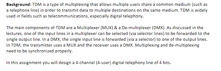
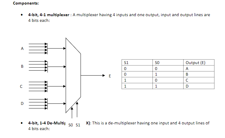
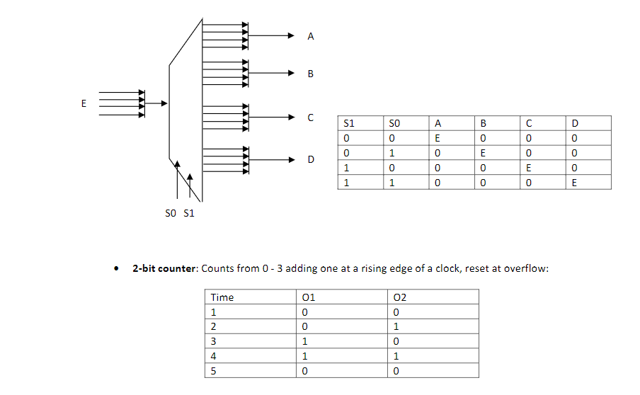
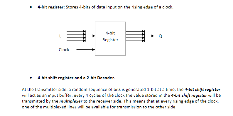
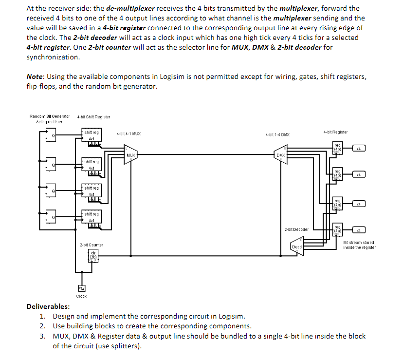
Background: TDM is a type of multiplexing that allows multiple users share a common medium (such as a telephone line) in order to transmit data to multiple destinations on the same medium. TDM is widely used in fields such as telecommunications, especially digital telephony. The main components of TDM are a Multiplexer (MUX) \& a De-multiplexer (DMX). As discussed in the lectures, one of the input lines in a multiplexer can be selected (via selector lines) to be forwarded to the single output line. In a DMX, the single input line is forwarded (via a selector) to one of the output lines. In TDM, the transmitter uses a MUX and the receiver uses a DMX. Multiplexing and de-multiplexing need to be synchronized properly. In this assignment you will design a 4-channel (4-user) digital telephony line of 4 bits. - 4-bit, 4-1 multiplexer : A multiplexer having 4 inputs and one output, input and output lines are 4 bits each: - 4-bit, 1-4 De-Multip so S1 X): This is a de-multiplexer having one input and 4 output lines of 4 bits each: - 2-bit counter: Counts from 0 - 3 adding one at a rising edge of a clock, reset at overflow: - 4-bit register: Stores 4-bits of data input on the rising edge of a clock. - 4-bit shift register and a 2-bit Decoder. At the transmitter side: a random sequence of bits is generated 1-bit at a time, the 4-bit shift register will act as an input buffer; every 4 cycles of the clock the value stored in the 4-bit shift register will be transmitted by the multiplexer to the receiver side. This means that at every rising edge of the clock, one of the multiplexed lines will be available for transmission to the other side. At the receiver side: the de-multiplexer receives the 4 bits transmitted by the multiplexer, forward the received 4 bits to one of the 4 output lines according to what channel is the multiplexer sending and the value will be saved in a 4-bit register connected to the corresponding output line at every rising edge of the clock. The 2-bit decoder will act as a clock input which has one high tick every 4 ticks for a selected 4-bit register. One 2-bit counter will act as the selector line for MUX,DMX \& 2-bit decoder for synchronization. Note: Using the available components in Logisim is not permitted except for wiring, gates, shift registers, flip-flops, and the random bit generator. Deliverables: 1. Design and implement the corresponding circuit in Logisim. 2. Use building blocks to create the corresponding components. 3. MUX, DMX \& Register data \& output line should be bundled to a single 4-bit line inside the block of the circuit (use splitters)
Step by Step Solution
There are 3 Steps involved in it

Get step-by-step solutions from verified subject matter experts