

Question: Design and implement the following function using combinatorial digital circuits using gates and logic components such as multiplexers and decoders. ( ULO 1 ) [
Design and implement the following function using combinatorial digital circuits using gates
and logic components such as multiplexers and decoders.
ULO Marks
A Design the output KMap
ULO Marks
B Design the output truthtable
ULO Marks
C Sketch the final design implementation circuit
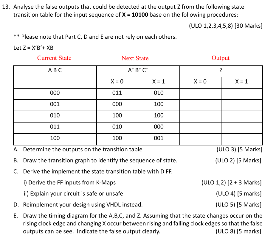
ULO MarksAnalyse the false outputs that could be detected at the output from the following state
transition table for the input sequence of base on the following procedures:
ULO Marks
Please note that Part C D and are not rely on each others.
Let
Current State
Next State
Output
A Determine the outputs on the transition table
ULO Marks
B Draw the transition graph to identify the sequence of state.
ULO Marks
C Derive the implement the state transition table with D FF
i Derive the FF inputs from KMaps
ULO Marks
ii Explain your circuit is safe or unsafe
ULO marks
D Reimplement your design using VHDL instead.
ULO Marks
E Draw the timing diagram for the and Assuming that the state changes occur on the
rising clock edge and changing occur between rising and falling clock edges so that the false
outputs can be see. Indicate the false output clearly.
ULO marks
Step by Step Solution
There are 3 Steps involved in it
1 Expert Approved Answer
Step: 1 Unlock

Question Has Been Solved by an Expert!
Get step-by-step solutions from verified subject matter experts
Step: 2 Unlock
Step: 3 Unlock