

Question: Design the logic to implement a Finite State Machine that counts in the sequence {0,2,4,6,9,12,0,2, 4,6,9,12,} Show how you would implement this design in a
Design the logic to implement a Finite State Machine that counts in the
sequence {0,2,4,6,9,12,0,2, 4,6,9,12,}
Show how you would implement this design in a PALCE16V8 type of
device.
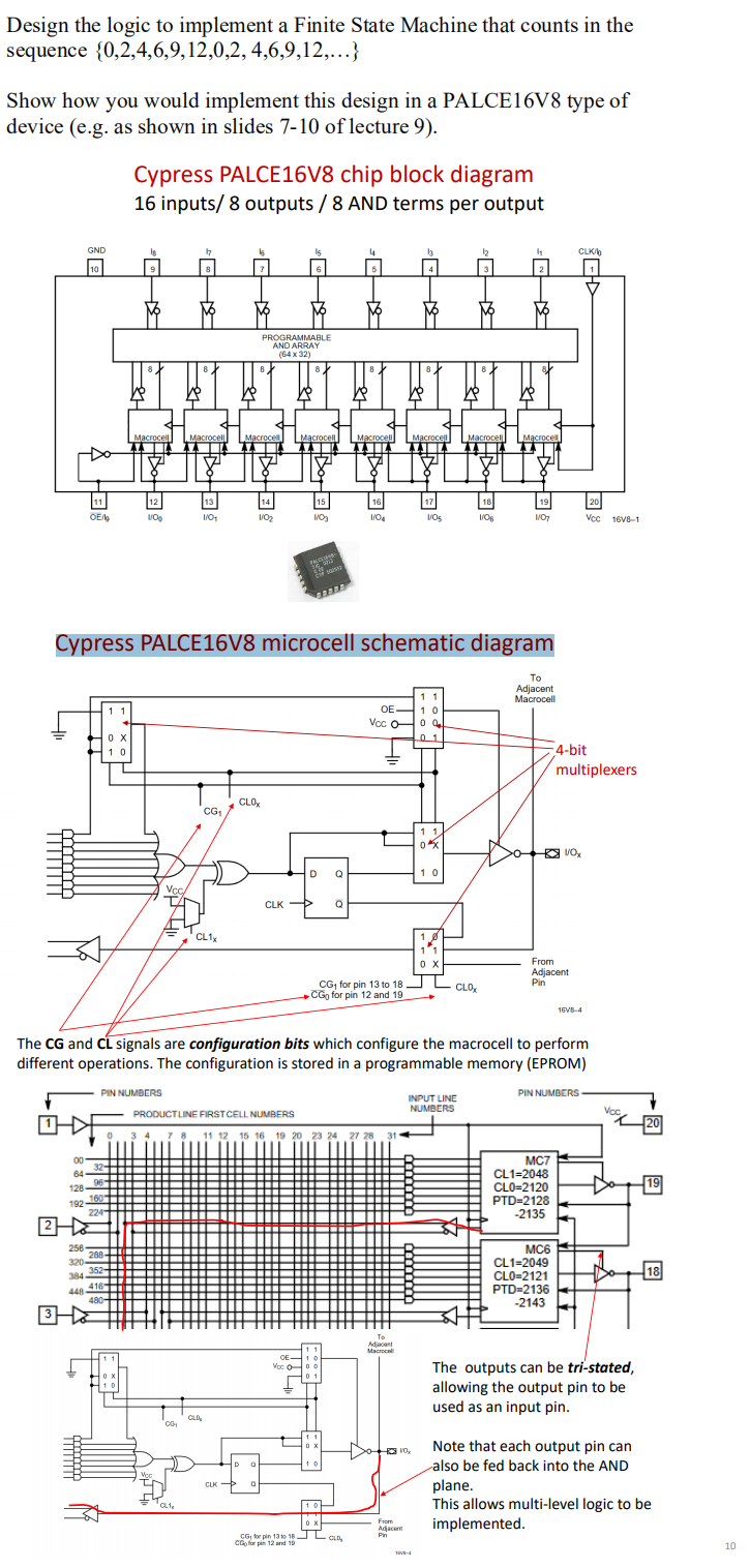
Design the logic to implement a Finite State Machine that counts in the sequence {0,2,4,6,9,12,0,2,4,6,9,12,...} Show how you would implement this design in a PALCE16V8 type of device (e.g. as shown in slides 7-10 of lecture 9). Cypress PALCE16V8 chip block diagram 16 inputs/ 8 outputs / 8 AND terms per output MAS GND Is th 4 10 9 5 PROGRAMMABLE AND ARRAY (64X32) VY Macrocell Macrocell Macrocell Macrocell Macrocell Made! TTT 7 7 2 X 12 CLK Macrocell Macrocell IL 11 12 14 13 1/01 15 1103 16 1/04 17 VOS 18 1/08 19 107 20 Vcc 16V8-1 OER VO VO2 Cypress PALCE16V8 microcell schematic diagram To Adjacent Macrocell 11 OE 10 Voc 0-0 0 0 0 x 10 -4-bit multiplexers CLOX CG 1 1 0 x VOX D Q 10 Voc/ CLK Q AT CL1 11 From Adjacent Pin CG for pin 13 to 18 CGo for pin 12 and 19 CLOX 165-4 The CG and CL signals are configuration bits which configure the macrocell to perform different operations. The configuration is stored in a programmable memory (EPROM) PIN NUMBERS PIN NUMBERS INPUT LINE NUMBERS PRODUCTLINE FIRSTCELL NUMBERS Voc 1 420 0 4 7 8 11 12 15 16 19 20 23 24 27 28 31 00 64 32- MC7 CL1=2048 CL0=2120 PTD=2128 -2135 128 192 224 19 2 256 288 320 352- 384 416 480 18 MC6 CL1=2049 CL0-2121 PTD=2136 -2143 Adjacent Mac CE Voc OOO 0 1 OX The outputs can be tri-stated, allowing the output pin to be used as an input pin. CLO, 00 D Q Voc CLK Note that each output pin can also be fed back into the AND plane. This allows multi-level logic to be implemented. 10 From Adjacent Pin T - CG for pin 1311 Go for pis 12 and 10 LLO, 10 Design the logic to implement a Finite State Machine that counts in the sequence {0,2,4,6,9,12,0,2,4,6,9,12,...} Show how you would implement this design in a PALCE16V8 type of device (e.g. as shown in slides 7-10 of lecture 9). Cypress PALCE16V8 chip block diagram 16 inputs/ 8 outputs / 8 AND terms per output MAS GND Is th 4 10 9 5 PROGRAMMABLE AND ARRAY (64X32) VY Macrocell Macrocell Macrocell Macrocell Macrocell Made! TTT 7 7 2 X 12 CLK Macrocell Macrocell IL 11 12 14 13 1/01 15 1103 16 1/04 17 VOS 18 1/08 19 107 20 Vcc 16V8-1 OER VO VO2 Cypress PALCE16V8 microcell schematic diagram To Adjacent Macrocell 11 OE 10 Voc 0-0 0 0 0 x 10 -4-bit multiplexers CLOX CG 1 1 0 x VOX D Q 10 Voc/ CLK Q AT CL1 11 From Adjacent Pin CG for pin 13 to 18 CGo for pin 12 and 19 CLOX 165-4 The CG and CL signals are configuration bits which configure the macrocell to perform different operations. The configuration is stored in a programmable memory (EPROM) PIN NUMBERS PIN NUMBERS INPUT LINE NUMBERS PRODUCTLINE FIRSTCELL NUMBERS Voc 1 420 0 4 7 8 11 12 15 16 19 20 23 24 27 28 31 00 64 32- MC7 CL1=2048 CL0=2120 PTD=2128 -2135 128 192 224 19 2 256 288 320 352- 384 416 480 18 MC6 CL1=2049 CL0-2121 PTD=2136 -2143 Adjacent Mac CE Voc OOO 0 1 OX The outputs can be tri-stated, allowing the output pin to be used as an input pin. CLO, 00 D Q Voc CLK Note that each output pin can also be fed back into the AND plane. This allows multi-level logic to be implemented. 10 From Adjacent Pin T - CG for pin 1311 Go for pis 12 and 10 LLO, 10
Step by Step Solution
There are 3 Steps involved in it

Get step-by-step solutions from verified subject matter experts