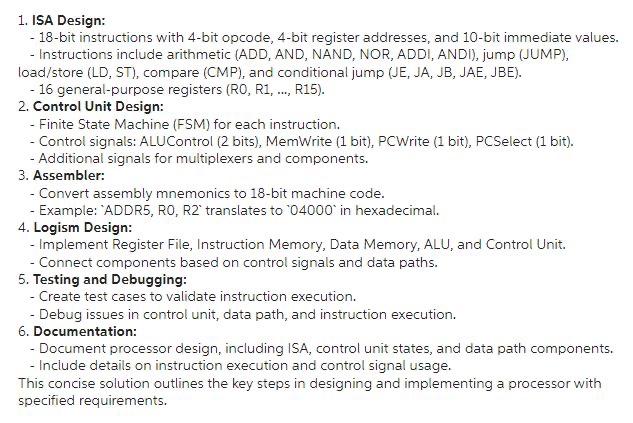
Question: digital logic design please help 1. ISA Design: - 18-bit instructions with 4-bit opcode, 4-bit register addresses, and 10-bit immediate values. - Instructions include arithmetic

1. ISA Design: - 18-bit instructions with 4-bit opcode, 4-bit register addresses, and 10-bit immediate values. - Instructions include arithmetic (ADD, AND, NAND, NOR, ADDI, ANDI), jump (JUMP), load/store (LD, ST), compare (CMP), and conditional jump (JE, JA, JB, JAE, JBE). - 16 general-purpose registers (R0, R1, ..., R15). 2. Control Unit Design: - Finite State Machine (FSM) for each instruction. - Control signals: ALUControl ( 2 bits), MemWrite ( 1 bit), PCWrite ( 1 bit), PCSelect ( 1 bit). - Additional signals for multiplexers and components. 3. Assembler: - Convert assembly mnemonics to 18 -bit machine code. - Example: 'ADDR5, R0, R2' translates to '04000' in hexadecimal. 4. Logism Design: - Implement Register File, Instruction Memory, Data Memory, ALU, and Control Unit. - Connect components based on control signals and data paths. 5. Testing and Debugging: - Create test cases to validate instruction execution. - Debug issues in control unit, data path, and instruction execution. 6. Documentation: - Document processor design, including ISA, control unit states, and data path components. - Include details on instruction execution and control signal usage. This concise solution outlines the key steps in designing and implementing a processor with specified requirements
Step by Step Solution
There are 3 Steps involved in it

Get step-by-step solutions from verified subject matter experts


