Question: Objectives: - Designing a Single-Cycle Processor with 16-bit instructions and 16-bit registers - Using the Logisim simulator to model and test the processor - Teamwork
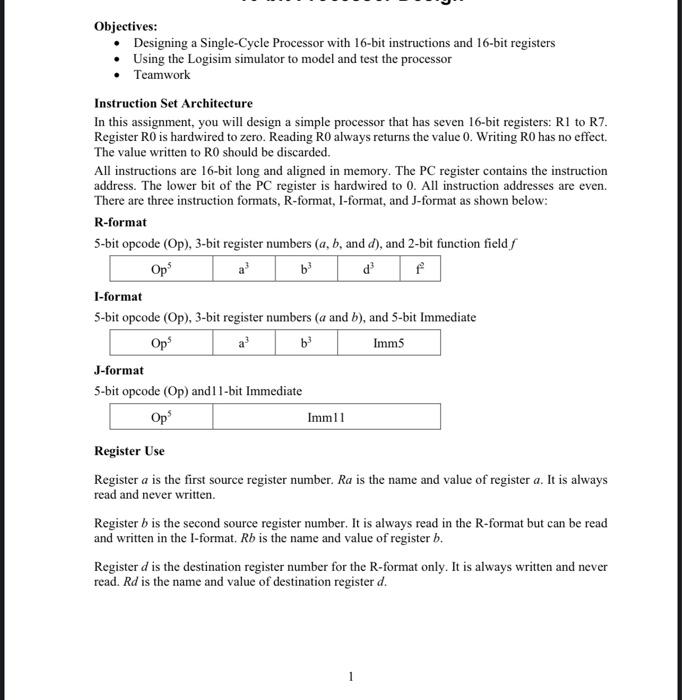
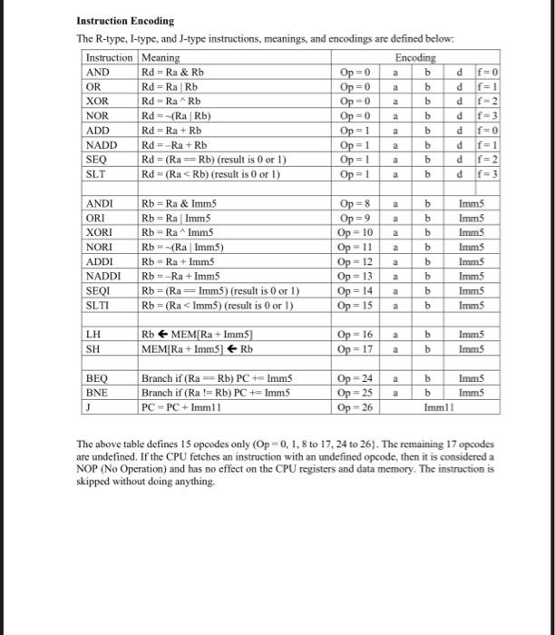
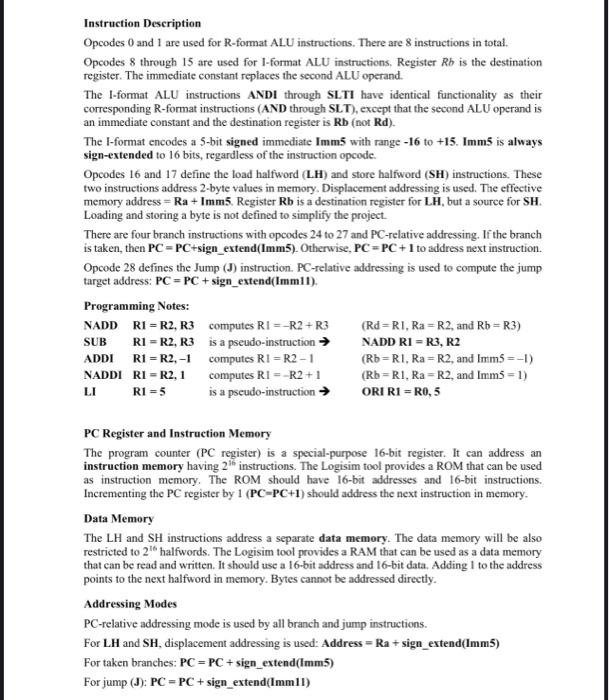
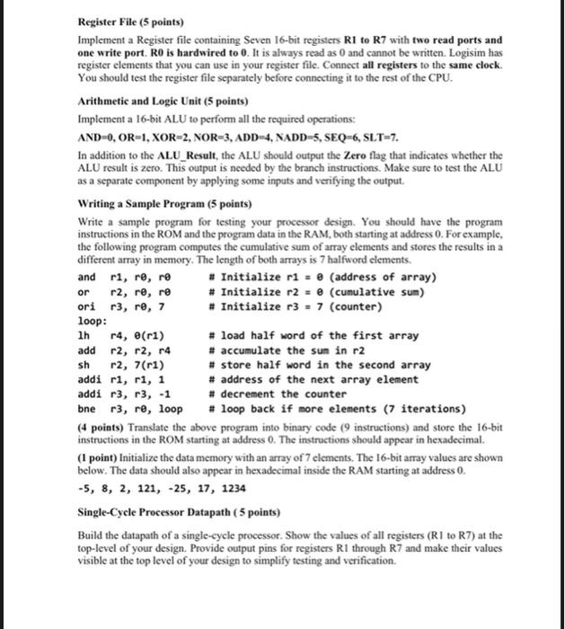
Objectives: - Designing a Single-Cycle Processor with 16-bit instructions and 16-bit registers - Using the Logisim simulator to model and test the processor - Teamwork Instruction Set Architecture In this assignment, you will design a simple processor that has seven 16-bit registers: R1 to R7. Register R0 is hardwired to zero. Reading R0 always returns the value 0 . Writing R0 has no effect. The value written to R0 should be discarded. All instructions are 16-bit long and aligned in memory. The PC register contains the instruction address. The lower bit of the PC register is hardwired to 0 . All instruction addresses are even. There are three instruction formats, R-format, I-format, and J-format as shown below: R-format 5-bit opcode (Op), 3-bit register numbers (a,b, and d), and 2-bit function field f I-format 5-bit opcode (Op), 3-bit register numbers ( a and b ), and 5-bit Immediate J-format 5-bit opcode (Op) and 11-bit Immediate Register Use Register a is the first source register number. Ra is the name and value of register a. It is always read and never written. Register b is the second source register number. It is always read in the R-format but can be read and written in the I-format. Rb is the name and value of register b. Register d is the destination register number for the R-format only. It is always written and never read. Rd is the name and value of destination register d. Instruction Encoding Tha D The above table defines 15 opcodes only (Op=0,1,8 to 17, 24 to 26). The remaining 17 opcodes are undefined. If the CPU fetches an instruction with an undefined opcode, then it is considered a NOP (No Operation) and has no effect on the CPU registers and data memory. The instruction is skipped without doing anything. Instruction Description Opcodes 0 and 1 are used for R-format ALU instructions. There are 8 instructions in total. Opcodes 8 through 15 are used for I-format ALU instructions. Register Rb is the destination register. The immediate constant replaces the second ALU operand. The I-format ALU instructions ANDI through SLTI have identical functionality as their corresponding R-format instructions (AND through SLT), except that the second ALU operand is an immediate constant and the destination register is Rb (not Rd ). The I-format encodes a 5 -bit signed immediate Imm5 with range 16 to +15. Imm5 is always sign-extended to 16 bits, regardless of the instruction opcode. Opcodes 16 and 17 define the load halfword (L.H) and store halfword (SH) instructions. These two instructions address 2 -byte values in memory. Displacement addressing is used. The effective memory address =Ra+ Imm5. Register Rb is a destination register for LH, but a source for SH. Loading and storing a byte is not defined to simplify the project. There are four branch instructions with opcodes 24 to 27 and PC-relative addressing. If the branch is taken, then PC=PC+ sign_extend(Imm5). Otherwise, PC=PC+1 to address next instruction. Opcode 28 defines the Jump (J) instruction. PC-relative addressing is used to compute the jump target address: PC=PC+ sign_extend(Imm11). Programming Notes: NADD R1=R2,R3 computes RI=R2+R3(Rd=R1,Ra=R2, and Rb=R3) SUB R=R2,R3 is a pseudo-instruction NADD RI=R3,R2 ADDI R=R2,1 computes RI=R21(Rb=R1,Ra=R2, and mmm5=1 ) NADDI R I =R2,1 computes RI=R2+1(Rb=R1,Ra=R2, and Imm5=1 ) LI RI=5 is a pscudo-instruction ORI R1 =R0,5 PC Register and Instruction Memory The program counter ( PC register) is a special-purpose 16-bit register. It can address an instruction memory having 2th instructions. The Logisim tool provides a ROM that can be used as instruction memory. The ROM should have 16-bit addresses and 16-bit instructions. Incrementing the PC register by 1(PC=PC+1) should address the next instruction in memory. Data Memory The LH and SH instructions address a separate data memory. The data memory will be also restricted to 216 halfwords. The Logisim tool provides a RAM that can be used as a data memory that can be read and written. It should use a 16-bit address and 16-bit data. Adding 1 to the address points to the next halfword in memory. Bytes cannot be addressed directly. Addressing Modes PC-relative addressing mode is used by all branch and jump instructions. For LH and SH, displacement addressing is used: Address = Ra + sign_extend(Imm5) For taken branches: PC=PC+ sign_extend (Imm5) For jump (J): PC=PC+ sign_extend(Imm II) Register File (5 points) Implement a Register file containing Seven 16-bit registers R1 to R7 with two read ports and one write port. R0 is hardwired to 0 . It is always read as 0 and cannot be written. Logisim has register elements that you can use in your register file. Connect all registers to the same clock. You should test the register file separately before connecting it to the rest of the CPU. Arithmetic and Logic Unit (5 points) Implement a 16-bit ALU to perform all the required operations: AND=0,OR=1,XOR=2,NOR=3,ADD=4,NADD=5,SEQ=6,SLT=7. In addition to the AL.U_Result, the ALU should output the Zero flag that indicates whether the ALU result is zero. This output is needed by the branch instructions. Make sure to test the ALU as a separate component by applying some inputs and verifying the output. Writing a Sample Program (5 points) Write a sample program for testing your processor design. You should have the program instructions in the ROM and the program data in the RAM, both starting at address 0 . For example, the following program computes the cumulative sum of array elements and stores the results in a different array in memory. The length of both arrays is 7 halfword elements. and r1,r,r * Initialize r1= (address of array) or r2,r,r \# Initialize r2= (cumulative sum) ori r3,r,7 \# Initialize r3=7 (counter) loop: Ih r4,(r1) I load half word of the first array add r2,r2,r4# accumulate the sun in r2 sh r2,7(r1) \# store half word in the second array addi r1,r1,1# address of the next array element addi r3,r3,1 I decrement the counter bne r3,r9, loop \# loop back if more elements (7 iterations) (4 points) Translate the above program into binary code ( 9 instructions) and store the 16-bit instructions in the ROM starting at address 0 . The instructions should appear in hexadecimal. (1 point) Initialize the data memory with an array of 7 elements. The 16-bit array values are shown below. The data should also appear in hexadecimal inside the RAM starting at address 0 . 5,8,2,121,25,17,1234 Single-Cycle Processor Datapath ( 5 points) Build the datapath of a single-cycle processor. Show the values of all registers (RI to R7) at the top-level of your design. Provide output pins for registers R1 through R7 and make their values visible at the top level of your design to simplify testing and verification. Control Logic (5 points) Implement the main control logic that should output all the main control signals according to the opcode value (2 points). Implement the ALU control logic that will output the ALU operation according to the opcode and function (2 points). Implement the PC control logic that will output the PCSre signal to implement the Jump and branch instructions correctly (1 point). Testing and Verification (10 points) To demonstrate that your CPU is working properly, you should do the following: 1. (5 points) Execute the sample program shown above and verify that it will compute correct results in the data memory. Draw a table that shows the final content of registers and the updated memory locations after completing the loop execution. Use the clock to synchronize the processor, update the program counter, the content of registers, and the data memory. 2. (5 points) Add more instructions in the ROM to verify the correctness of ALL instructions. Draw a table that shows each instruction in assembly language and in hexadecimal, the content of the updated register, memory location for SH, or the PC register for a branch or jump. You should have an entry in the table for cach instruction that you tested in the instruction set. Project Report (10 points) The report document must contain sections highlighting the following: 1 - Design and Implementation (5 points) - Provide drawings of the various components and the overall datapath. You can take screen snapshots and include them in your document. - Provide a complete description of the control logic and the control signals. Provide a table giving the control signal values for each instruction. 2 - Simulation and Testing (5 points) - Describe the test programs that you used to test your design with sufficient comments describing the instructions, updated registers, and memory locations. Provide a table that shows the expected results in registers or data stored in memory. Compare the expected results against the actual results produced by your processor design. List all the instructions that were tested and worked correctly. List all the instructions that did not run properly. - Provide snapshots showing test programs and their output results. 3-Teamwork - Two or at most three students can form a group. Write the names of all the group members on the project report title page. - Group members are required to coordinate their work among themselves, so that everyone is involved in design, implementation, simulation, and testing. Submit the Logisim circuits and the project report document on Blackboard