

Question: Digital Principles - UFMFF 8 - 3 0 - 1 Small - Scale Project Design Problem specification: To design and implement a computer system, central
Digital Principles UFMFF
SmallScale Project
Design Problem specification:
To design and implement a computer system, central processing unit is considered as the vital component. It has two major components, the control unit, and the arithmetic logic unit ALU You are required to complete the following tasks.
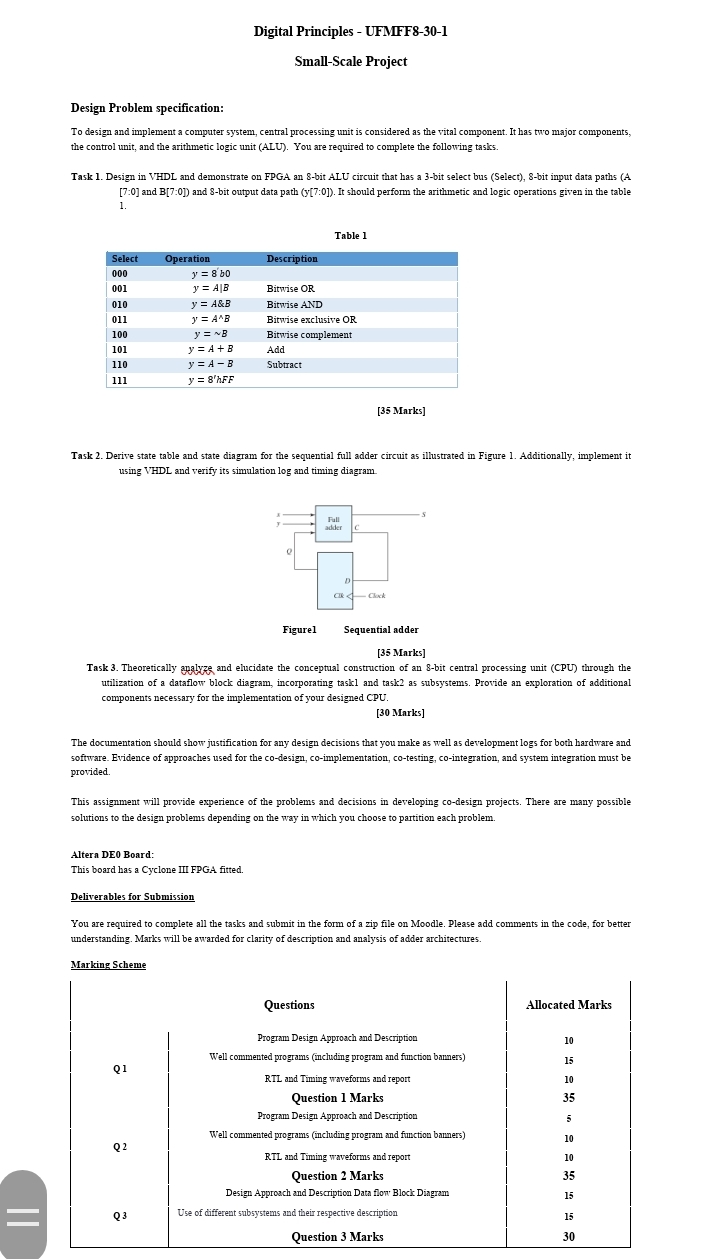
Task Design in VHDL and demonstrate on FPGA an bit ALU circuit that has a bit select bus Selectbit input data paths A : and : and bit output data path y: It should perform the arithmetic and logic operations given in the table
Table
tableSelectOperation,DescriptionBitwise OR&Bitwise ANDBitwise exclusive ORBitwise complementAddSubtract
Marks
Task Derive state table and state diagram for the sequential full adder circuit as illustrated in Figure Additionally, implement it using VHDL and verify its simulation log and timing diagram.
Marks
Task Theoretically analyze and elucidate the conceptual construction of an bit central processing unit CPU through the utilization of a dataflow block diagram, incorporating taskl and task as subsystem Provide an exploration of additional components necessary for the implementation of your designed CPU.
Marks
The documentation should show justification for any design decisions that you make as well as development logs for both hardware and software. Evidence of approaches used for the codesign, coimplementation, cotesting, cointegration, and system integration must be provided.
This assignment will provide experience of the problems and decisions in developing codesign projects. There are many possible solutions to the design problems depending on the way in which you choose to partition each problem.
Altera DE Board:
This board has a Cyclone III FPGA fitted.
Deliverables for Submission
You are required to complete all the tasks and submit in the form of a zip file on Moodle. Please add comments in the code, for better understanding. Marks will be awarded for clarity of description and analysis of adder architectures.
Marking Scheme
Questions
Program Design Approach and Description
Program Design Approach and Description
RTL and Timing waveforms and report
Question Marks
Program Design Approach and Description
Well commented programs including program and fumction bamners
RTL and Timing waveforms and report
Question Marks
Design Approach and Description Data flow Block: Dingram
Use of different subsystems and their respective description
Allocated Marks
Step by Step Solution
There are 3 Steps involved in it
1 Expert Approved Answer
Step: 1 Unlock

Question Has Been Solved by an Expert!
Get step-by-step solutions from verified subject matter experts
Step: 2 Unlock
Step: 3 Unlock