

Question: Distributed Matching Network Design OBJECTIVE: BUILD MATCHING NETWORKS FOR A NE 6 6 1 MO 4 DEVICE AT 3 GHZ BY REPLACING THE ATF 5
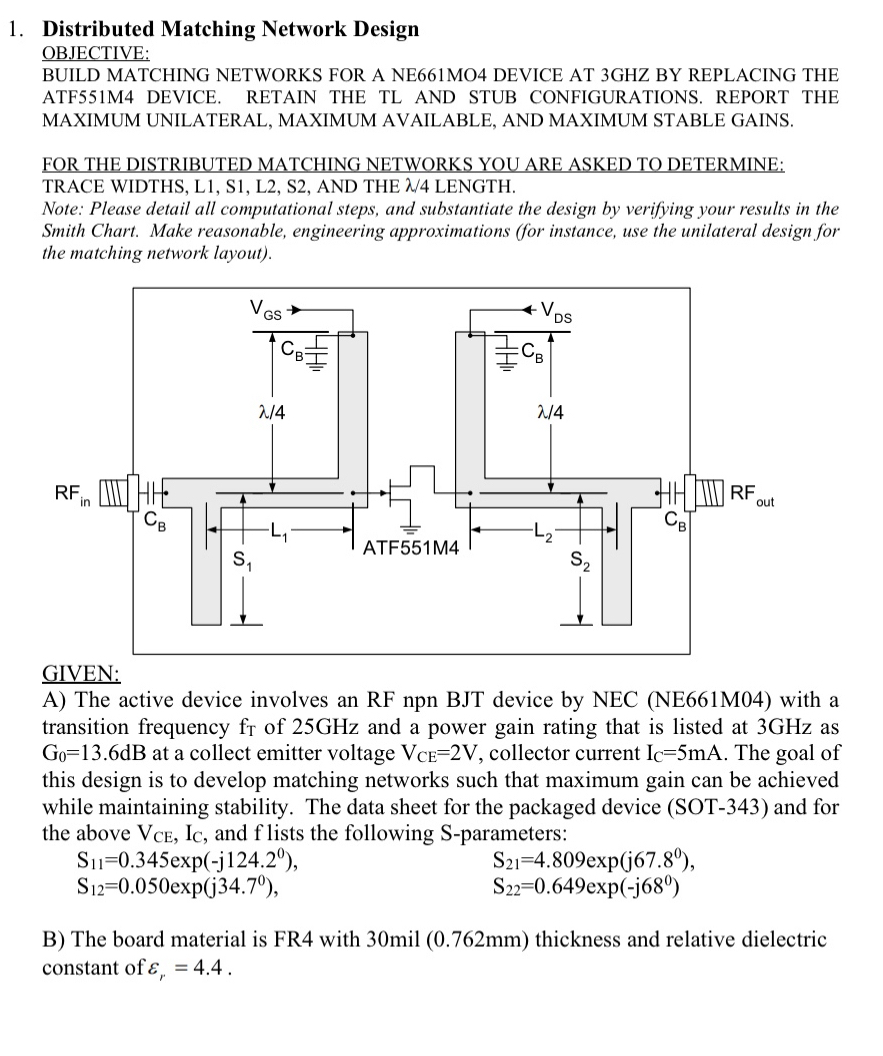
Distributed Matching Network Design
OBJECTIVE:
BUILD MATCHING NETWORKS FOR A NEMO DEVICE AT GHZ BY REPLACING THE ATFM DEVICE. RETAIN THE TL AND STUB CONFIGURATIONS. REPORT THE MAXIMUM UNILATERAL, MAXIMUM AVAILABLE, AND MAXIMUM STABLE GAINS.
FOR THE DISTRIBUTED MATCHING NETWORKS YOU ARE ASKED TO DETERMINE: TRACE WIDTHS, L S L S AND THE LENGTH.
Note: Please detail all computational steps, and substantiate the design by verifying your results in the Smith Chart. Make reasonable, engineering approximations for instance, use the unilateral design for the matching network layout
GIVEN:
A The active device involves an RF npn BJT device by NEC NEM with a transition frequency of GHz and a power gain rating that is listed at GHz as at a collect emitter voltage collector current The goal of this design is to develop matching networks such that maximum gain can be achieved while maintaining stability. The data sheet for the packaged device SOT and for the above and f lists the following Sparameters:
expexp
expexp
B The board material is FR with mil thickness and relative dielectric constant of
Step by Step Solution
There are 3 Steps involved in it
1 Expert Approved Answer
Step: 1 Unlock

Question Has Been Solved by an Expert!
Get step-by-step solutions from verified subject matter experts
Step: 2 Unlock
Step: 3 Unlock