

Question: don't need to do the test bench file, only mux and gates Prelab Work Write a behavioral model (22-ns delay) of a 4-bit bidirectional universal
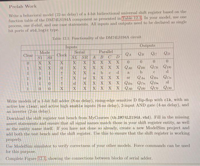
Prelab Work Write a behavioral model (22-ns delay) of a 4-bit bidirectional universal shift register based on the function table of the DM74ALS191A component as presented in Table 12.1 In your model, use one process, one if-elsif, and one case statements. All inputs and outputs need to be declared as single bit ports of std logic type. Table 12.1: Functionality of the DM74LS194A circuit Clear 0 1 Mode SI SO X X X X 1 1 0 1 1 0 0 0 Inputs Outputs Serial Parallel Clock QB Q QD SL SR A B C D X X X X X X X 0 0 0 0 0 X X x x x x Q Q Qco Qoo X b d a b d X Sr X X X X ST QAn QBn Qen 1 X X X X X QBn Qon QDn sl X X X X X X QAO Q30 Qco QDO 2 1 Write models of a l-bit full adder (8-ns delay), rising-edge sensitive D flip-flop with clk, with an active low clear, and active high enable inputs (6-ns delay), 2-input AND gate (1-nis delay), and an inverter (2-ns delay), Download the shift register test bench from MyCourses (tb DM74LS1941.vhd). Fill in the missing assert statements and ensure that all signal names match those in your shift register entity, as well as the entity name itself. If you have not done so already, create a new ModelSim project and add both the test bench and the shift register. Use this to ensure that the shift register is working properly. Use ModelSim simulator to verify correctness of your other models. Force commands can be used for this purpose. Complete Figure 12.11 showing the connections between blocks of serial adder. Prelab Work Write a behavioral model (22-ns delay) of a 4-bit bidirectional universal shift register based on the function table of the DM74ALS191A component as presented in Table 12.1 In your model, use one process, one if-elsif, and one case statements. All inputs and outputs need to be declared as single bit ports of std logic type. Table 12.1: Functionality of the DM74LS194A circuit Clear 0 1 Mode SI SO X X X X 1 1 0 1 1 0 0 0 Inputs Outputs Serial Parallel Clock QB Q QD SL SR A B C D X X X X X X X 0 0 0 0 0 X X x x x x Q Q Qco Qoo X b d a b d X Sr X X X X ST QAn QBn Qen 1 X X X X X QBn Qon QDn sl X X X X X X QAO Q30 Qco QDO 2 1 Write models of a l-bit full adder (8-ns delay), rising-edge sensitive D flip-flop with clk, with an active low clear, and active high enable inputs (6-ns delay), 2-input AND gate (1-nis delay), and an inverter (2-ns delay), Download the shift register test bench from MyCourses (tb DM74LS1941.vhd). Fill in the missing assert statements and ensure that all signal names match those in your shift register entity, as well as the entity name itself. If you have not done so already, create a new ModelSim project and add both the test bench and the shift register. Use this to ensure that the shift register is working properly. Use ModelSim simulator to verify correctness of your other models. Force commands can be used for this purpose. Complete Figure 12.11 showing the connections between blocks of serial adder
Step by Step Solution
There are 3 Steps involved in it

Get step-by-step solutions from verified subject matter experts