

Question: 7.2 Datapath Design To achieve the signed binary number multiplication based on the Booth's algorithm, datapath requires certain logic blocks including; three 4-bit registers to
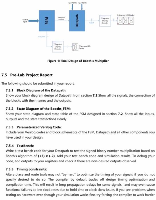
7.2 Datapath Design To achieve the signed binary number multiplication based on the Booth's algorithm, datapath requires certain logic blocks including; three 4-bit registers to store and an arithmetic shift right M, A and Q values and a 1-bit register to store and an arithmetic shift right Q.1 value. An ALU will be used to perform arithmetic operations (A+M/A-M) and a down counter to keep track of the number of operations of FSM based on the number of bits that the datapath is designed for. This design should follow a parametric model so that the bit size of the multiplier can be adjusted. Firstly, use block diagram representation and design the datapath for Boot's Algorithm, then write a parameterized Verilog code to define your datapath. Only 4-bit-user inputs (M and Q) are external inputs to the datapath and the CLK, RST and the other control signals should come from the FSM. 7.3 FSM Design Control unit of this datapath will be implemented by the Booths FSM as described in the lectures. The multiplier control FSM will have three external input START, CLK and RST. Once a Start signal is received the Booth algorithm for multiplication process will start and will continue until n (number of bits) in the down counter = 0. Add an asynchronous RST signal and out_state signal to the design for debugging your FSM. FSM prepared in Experiment 6 can help you to implement Booths_FSM. Draw the state diagram for the FSM showing all the inputs, outputs, and the state transitions clearly. 7.4 Top-Level Design: When the two core parts of Booth's multiplier design is done, connect the block in a top-level design as depicted in Figure 1. This top-level implementation will be programmed into your FPGA Board. You will use three displays for the outputs where one of the displays on the left will show which state the FSM is in. 7.Segment Duh FSM Datapath 7-segment Display Decoder elgta 75D Dha Decoder Figure 1: Final Design of Booth's Multiplier 7.5 Pre-Lab Project Report The following should be submitted in your report 7.5.1 Block Diagram of the Datapath: Show your block diagram design of Datapath from section 7.2 Show all the signals, the connection of the blocks with their names and the outputs. 7.5.2 State Diagram of the Booths_FSM: Show your state diagram and state table of the FSM designed in section 7.2. Show all the inputs, outputs and the state transactions clearly. 7.5.3 Parameterized Verilog Code: Include your Verilog codes and block schematics of the FSM, Datapath and all other components you have used in your design 7.5.4 TestBench: Write a test bench code for your Datapath to test the signed binary number multiplication based on Booth's algorithm of (+3) (-2). Add your test bench code and simulation results. To debug your code, add outputs to your registers and check if there are non-desired outputs observed. 7.5.5 Timing constraints: Altera place and route tools may not "try hard" to optimize the timing of your signals if you do not specify desired to do so. The compiler by default trades off design timing optimization and compilation time. This will result in long propagation delays for some signals, and may even cause functional failures at low clock rates due to hold time or clock skew issues. If you see problems when testing on hardware even though your simulation works fine, try forcing the compiler to work harder on timing optimization by going to Fitter (Place & Route) Edit Settings and marking "Optimize hold timing" as "All paths". In addition, mark "Fitter effort" as "Standard fit" and change "Desired worst-case slack" to 5 ns. You should not nominally have any path with a higher delay than 20ns. You can check the Fitter Timing analysis report after the compilation to make sure you do not have any timing violation (appears in red). If you have setup time problems, you can usually fix them by slowing down your system clock. For hold problems, or clock skew problems, the previous settings should help. 7.5.6 Report: Include your name, course name, course code, date, an objective statement, and a conclusion in your report. Add short comments to briefly explain each Verilog code, schematic and simulation that you submit. Once everything works well in simulations, check your timing analysis report to find out how fast your design is expected to work. Specify the fmax in your report and append a printed copy of the timing analysis summary to your report. 7.6 Experimental Work: Booth's Algorithm 7.6.1 Experimental Setup Verify to make sure your workbench has all of the following items: A Personal Computer (PC) with Altera Quartus II ISE 13.0 Project Navigator - DEO Demo Board with Cyclone III EP3C16F484C6 FPGA installed on a card with 10 input toggle switches, three pushbuttons, and four 7-Segment LED displays among other components A USB cable connected between the demo board and the PC using USB interface During your final demo, you will be evaluated on your understanding of: o Combinational and sequential concepts, Multiplier design details, o Verilog and schematic based design entry, and o Simulation flows. You will program your final design onto an FPGA and demonstrate it. If something goes wrong with the hardware demo or does not seem to work consistently using a manual clock (from push-button) or free-running on-board clock, you should be ready to do a quick post-route simulation of your design to demonstrate the corresponding functionality in simulation. (You can only do this if you understand your simulations very well.) Prepare various test bench waveforms in advance to be able to do this. Remember, you will have very limited time with the Teaching Assistant to demonstrate your working design, AND you fully understand your design. He/she will perform the debugging for you. Start your lab early so you can resolve any problems ahead of time during office hours, and come to the final demo fully prepared
Step by Step Solution
There are 3 Steps involved in it

Get step-by-step solutions from verified subject matter experts