

Question: Draw a timing diagram for each gate, showing the relationship between control input, signal input, and gate output, then complete the table given below relating
Draw a timing diagram for each gate, showing the relationship between control input, signal input, and gate output, then complete the table given below relating control input, signal input, and output for all the six gates (e.g., for an AND gate, Y = 0 when A = 0; Y = B when A = 1).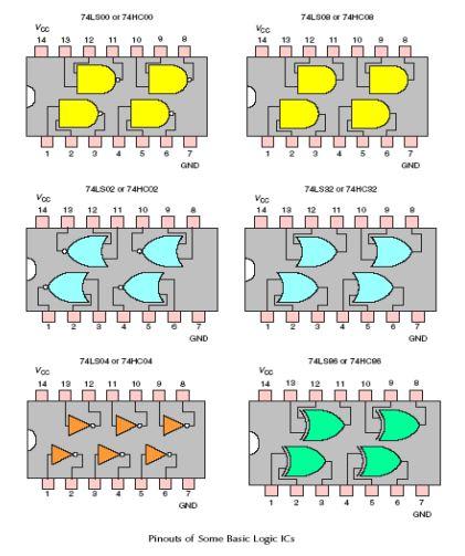
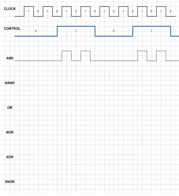
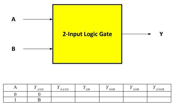
74L 500 ot 74HCOO 74L30E 74HCOB Voc 14 Vec 13 12 11 10 9 13 12 11 10 9 8 . 1 2 3 4 5 6 7 GND 1 2 3 4 5 6 7 GND 74LSCE or 74HCO 74882 or 74HC22 Voc 14 12 12 11 10 Voc 14 19 10 12 11 10 D . . 5 GND GND 74LSAS O 74HCOS 74LS04 or 74H004 Voc 14 13 12 11 10 9 8 13 12 11 10 8 18 9 GND 4 GND Pinouts of Some Basic Logics CLOCK 1 0 1 0 0 0 0 0 0 0 CONTROL 0 AND NAND OR NOR XOR XNOR A 2-Input Logic Gate Y B B Y AND NAND YOR Y NOR Y XOR Y XNOR A 0 1 0 B
Step by Step Solution
There are 3 Steps involved in it

Get step-by-step solutions from verified subject matter experts