

Question: ET_585 HOMEWORK_402 Problem_101) The input shown signal shown below is applied to an inverter. Draw a timing diagram showing the input and output. HIGH VN
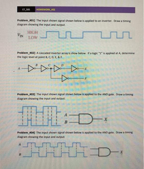
![HIGH VN LOW Problem_#02] A cascaded inverter array is show below. If](https://dsd5zvtm8ll6.cloudfront.net/si.experts.images/questions/2024/09/66f3e3480fbf7_46366f3e347971da.jpg)
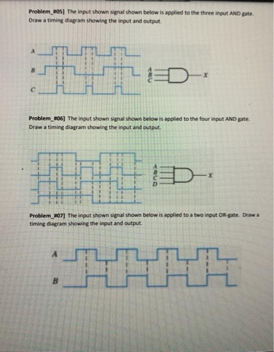
ET_585 HOMEWORK_402 Problem_101) The input shown signal shown below is applied to an inverter. Draw a timing diagram showing the input and output. HIGH VN LOW Problem_#02] A cascaded inverter array is show below. If a logic *1" is applied at A, determine the logic level at point B, C, D, E, & F. Problem_#03] The input shown signal shown below is applied to the AND gate. Drawa timing diagram showing the input and output. D-* B Problem_#04] The input shown signal shown below is applied to the AND gate. Draw a timing diagram showing the input and output H Problem_HS) The input shown signal shown below is applied to the three input AND gate. Draw a timing diagram showing the input and output. I Problem_406) The input shown signal shown below is applied to the four input AND gate. Draw a timing diagram showing the input and output. Problem_107] The input shown signal shown below is applied to a two input OR-gate. Drawa timing diagram showing the input and output. A B Problem_408) The input shown signal shown below is applied to the three input OR-gate Draw a timing diagram showing the input and output Problem_#09] The input shown signal shown below is applied to the four input OR gate. Draw a timing diagram showing the input and output Problem_110] The input shown signal shown below, draw a timing diagram showing the input and output C D
Step by Step Solution
There are 3 Steps involved in it

Get step-by-step solutions from verified subject matter experts