Question: During the 2nd midterm exam, Chris solved a problem on a new MOSFET device. Briefly, the semiconductor is a wide-bandgap material with the following material
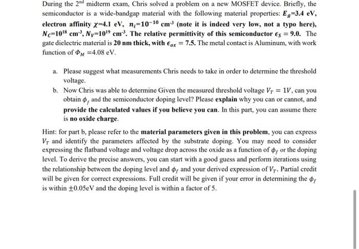
During the 2nd midterm exam, Chris solved a problem on a new MOSFET device. Briefly, the semiconductor is a wide-bandgap material with the following material properties: Eg=3.4eV, electron affinity =4.1eV,ni=1010cm3 (note it is indeed very low, not a typo here), NC=1018cm3,NV=1019cm3. The relative permittivity of this semiconductor S=9.0. The gate dielectric material is 20nm thick, with ox=7.5. The metal contact is Aluminum, with work function of M=4.08eV. a. Please suggest what measurements Chris needs to take in order to determine the threshold voltage. b. Now Chris was able to determine Given the measured threshold voltage VT=1V, can you obtain f and the semiconductor doping level? Please explain why you can or cannot, and provide the calculated values if you believe you can. In this part, you can assume there is no oxide charge. Hint: for part b, please refer to the material parameters given in this problem, you can express VT and identify the parameters affected by the substrate doping. You may need to consider expressing the flatband voltage and voltage drop across the oxide as a function of f or the doping level. To derive the precise answers, you can start with a good guess and perform iterations using the relationship between the doping level and f and your derived expression of VT. Partial credit will be given for correct expressions. Full credit will be given if your error in determining the f is within 0.05eV and the doping level is within a factor of 5 . During the 2nd midterm exam, Chris solved a problem on a new MOSFET device. Briefly, the semiconductor is a wide-bandgap material with the following material properties: Eg=3.4eV, electron affinity =4.1eV,ni=1010cm3 (note it is indeed very low, not a typo here), NC=1018cm3,NV=1019cm3. The relative permittivity of this semiconductor S=9.0. The gate dielectric material is 20nm thick, with ox=7.5. The metal contact is Aluminum, with work function of M=4.08eV. a. Please suggest what measurements Chris needs to take in order to determine the threshold voltage. b. Now Chris was able to determine Given the measured threshold voltage VT=1V, can you obtain f and the semiconductor doping level? Please explain why you can or cannot, and provide the calculated values if you believe you can. In this part, you can assume there is no oxide charge. Hint: for part b, please refer to the material parameters given in this problem, you can express VT and identify the parameters affected by the substrate doping. You may need to consider expressing the flatband voltage and voltage drop across the oxide as a function of f or the doping level. To derive the precise answers, you can start with a good guess and perform iterations using the relationship between the doping level and f and your derived expression of VT. Partial credit will be given for correct expressions. Full credit will be given if your error in determining the f is within 0.05eV and the doping level is within a factor of 5


